


 Dan's Biz Bookshelf: 'Revenge of the Tipping Point'
 Marcy's Musings: Engineering Economics
 Punching Out: Should You Sell Your Company to a Private Equity Firm?


Since the 1960s, computer chips have been built using a process called photolithography. But in the past five years, chip features have gotten smaller than the wavelength of light, which has required some ingenious modifications of photolithographic processes. Keeping up the rate of circuit miniaturization that we’ve come to expect — as predicted by Moore’s Law — will eventually require new manufacturing techniques.
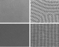
Block copolymers, molecules that spontaneously self-assemble into useful shapes, are one promising alternative to photolithography. In a new paper in the journal Nature Communications, MIT researchers describe the first technique for stacking layers of block-copolymer wires such that the wires in one layer naturally orient themselves perpendicularly to those in the layer below.
The ability to easily produce such “mesh structures” could make self-assembly a much more practical way to manufacture memory, optical chips, and even future generations of computer processors.
“There is previous work on fabricating a mesh structure — for example our work,” says Amir Tavakkoli, a postdoc in MIT’s Research Laboratory of Electronics and one of three first authors on the new paper. “We used posts that we had fabricated by electron-beam lithography, which is time consuming. But here, we don’t use the electron-beam lithography. We use the first layer of block copolymer as a template to self-assemble another layer of block copolymer on top of it.”
Tavakkoli’s co-first-authors on the paper are Sam Nicaise, a graduate student in electrical engineering, and Karim Gadelrab, a graduate student in materials science and engineering. The senior authors are Alfredo Alexander-Katz, the Walter Henry Gale Associate Professor of Materials Science and Engineering; Caroline Ross, the Toyota Professor of Materials Science and Engineering; and Karl Berggren, a professor of electrical engineering.
Page 1 of 3
Share on:


Suggested Items
CHIPS for America Announces Up to $300M in Funding to Boost U.S. Semiconductor Packaging
11/21/2024 | U.S. Chamber of CommerceThe Biden-Harris Administration announced that the U.S. Department of Commerce (DOC) is entering negotiations to invest up to $300 million in advanced packaging research projects in Georgia, California, and Arizona to accelerate the development of cutting-edge technologies essential to the semiconductor industry.
Global Citizenship: What I’ve Learned About the American PCB Business
11/20/2024 | Tom Yang -- Column: Global CitizenshipNavigating the complexities of the American PCB business has been an eye-opening experience. During my time in America, I have become more familiar with the American PCB business and doing business here. If I may, and with your indulgence, I would like to share my humble impressions of the American PCB industry and the American way of doing business, which I find interesting and admirable.
Spirit Announces Purchase Agreement with Tex Tech Industries for Intended Sale of FMI
11/19/2024 | Spirit AeroSystems, Inc.Spirit AeroSystems Holdings, Inc. announces a purchase agreement to sell Fiber Materials, Inc (FMI) business based in Biddeford, Maine, and Woonsocket, Rhode Island, to Tex-Tech Industries, Inc. for $165,000,000 in cash, subject to customary adjustment.
Ventec to Become Primary PCB Materials Supplier for Teltonika
11/13/2024 | VentecVentec International Group and high-tech design and manufacturing company Teltonika announce that Ventec is to become supply chain partner and primary supplier of PCB base materials to Teltonika, which is preparing to open a new PCB manufacturing plant at its base in Vilnius, Lithuania.
AIM to Present on Micro/MiniLED Applications at Hangjia Talk in Shenzhen, China
11/11/2024 | AIM SolderAIM Solder, a leading global manufacturer of solder assembly materials for the electronics industry, is pleased to announce its participation in the upcoming Hangjia annual industry event focused on the future of the LED display sector.