


 Dan’s Biz Bookshelf: Four Important Books You Need to Read (Not Just Say You Have)
 The Marketing Minute: Cracking the Code of Technical Marketing


Novel Nanotechnology Technique for Table-Top Production of Flat Optics
January 28, 2016 | University of IllinoisEstimated reading time: 2 minutes
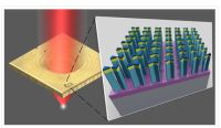
Researchers from the University of Illinois at Urbana-Champaign have developed a simplified approach to fabricating flat, ultrathin optics. The new approach enables simple etching without the use of acids or hazardous chemical etching agents.
“Our method brings us closer to making do-it-yourself optics a reality by greatly simplifying the design iteration steps,” explained Kimani Toussaint, an associate professor of mechanical science and engineering who led the research published this week in Nature Communications. “The process incorporates a nanostructured template that can be used to create many different types of optical components without the need to go into a cleanroom to make a new template each time a new optical component is needed.
“In recent years, the push to foster increased technological innovation and basic scientific and engineering interest from the broadest sectors of society has helped to accelerate the development of do-it-yourself (DIY) components, particularly those related to low-cost microcontroller boards,” Toussaint remarked. “Simplifying and reducing the steps between a basic design and fabrication is the primary attraction of DIY kits, but typically at the expense of quality. We present plasmon-assisted etching as an approach to extend the DIY theme to optics with only a modest tradeoff in quality, specifically, the table-top fabrication of planar optical components.”
“Our method uses the intuitive design aspects of diffractive optics by way of simple surface modification, and the electric-field enhancement properties of metal nanoantennas, which are typically the building blocks of metasurfaces,” stated Hao Chen, a former postdoctoral researcher in Toussaint’s lab and first author of the paper, “Towards do-it-yourself planar optical components using plasmon-assisted etching.”
According to Chen, laser light scans the template—a 2D array of gold pillar-supported bowtie nanoantennas (with an area of 80 x 80 square micrometers)—which is submerged in water, in a desired pattern in a microscope. The light-matter interaction, enhanced by the nanoantennas, produces a strong heating effect. As a result, the gold layer of the nanoantennas undergoes thermal expansion that works against its adhesion with their glass substrate. With certain amount of optical power, the force provided by thermal expansion allows the gold layer to break away from the substrate, etching the metal.
“Overall, the workload in cleanroom is greatly reduced,” Chen noted. “Once the template is ready, it is like a paper sheet. You can ‘draw’ all the optical elements you need on a ‘canvas’ using a conventional laser-scanning optical microscope.”
The study demonstrated fabrication of various ultra-thin (characteristic dimension less than the optical wavelength), flat optical components using the same template. The specific optical components fabricated by the researchers included a flat focusing lens (also known as a Fresnel zone plate) with focal length of ~150 micrometers, a diffraction grating, and a holographic converter that imparts angular momentum to a standard optical beam.
According to the researchers, the PAE method and specialized template could also be used to enable preferential trapping and sorting of particles, to create so-called optofluidic channels “without walls.”
Toussaint directs the PROBE laboratory in the Department of Mechanical Science and Engineering at Illinois. In addition to Toussaint and Chen, study co-authors include graduate student Qing Ding, former graduate student Abdul Bhuiya, and Harley T. Johnson, a professor of mechanical science and engineering at Illinois.
Share on:


Testimonial
"The I-Connect007 team is outstanding—kind, responsive, and a true marketing partner. Their design team created fresh, eye-catching ads, and their editorial support polished our content to let our brand shine. Thank you all! "
Sweeney Ng - CEE PCBSuggested Items
BLT Joins Microchip Partner Program as Design Partner
09/17/2025 | BUSINESS WIREBLT, a U.S.-owned and operated engineering design services firm announced it has joined the Microchip Design Partner Program.
HyRel Technologies Showcases Summer Intern Success Through Hands-On Innovation
09/16/2025 | HyRel TechnologiesHyRel Technologies, a global provider of quick turn semiconductor modification solutions, proudly highlights the accomplishments of its two recent summer interns, Danny Hoang and Nisarg Jadav.
ASM Technologies Limited signs MoU with the Guidance, Government of Tamilnadu to Expand Design-Led Manufacturing capabilities for ESDM
09/15/2025 | ASM TechnologiesASM Technologies Limited, a pioneer in Design- Led Manufacturing in the semiconductor and automotive industries, announced signing of Memorandum of Understanding (MoU) with the Guidance, Government of Tamilnadu whereby it will invest Rs. 250 crores in the state to expand its ESDM related Design-Led Manufacturing and precision engineering capacity. ASM Technologies will acquire 5 acres of land from the Government of Tamilnadu to set up a state-of-the-art design facility in Tamil Nadu's growing technology manufacturing ecosystem, providing a strong strategic advantage and long-term benefits for ASM.
Intel Announces Key Leadership Appointments to Accelerate Innovation and Strengthen Execution
09/09/2025 | Intel CorporationIntel Corporation today announced a series of senior leadership appointments that support the company’s strategy to strengthen its core product business, build a trusted foundry, and foster a culture of engineering across the business.
Cadence to Acquire Hexagon’s Design & Engineering Business
09/08/2025 | Cadence Design SystemsCadence announced it has entered into a definitive agreement to acquire the Design & Engineering (D&E) business of Hexagon AB, which includes its MSC Software business—a pioneer in engineering simulation and analysis solutions.