


 Dan’s Biz Bookshelf: ‘Elevate: Push Beyond Your Limits'
 The Marketing Minute: The First Step to More Sales—Marketing
 It’s Only Common Sense: Customer Service Is Sales in Disguise


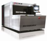
L&M Imaging Systems Appointed as the Distributor for Altix Automa-Tech Products in the UK and Ireland
February 3, 2016 | L&M Imaging SystemsEstimated reading time: 1 minute
L&M Imaging Systems announced the addition of direct imaging solutions for the printed circuit board and photo chemical machining applications.
According to Tim Clough, Managing Director of L&M, "The introduction of the Altix range of products adds a new range of imaging technologies to our existing printing products. This is an exciting change in direction for L&M. The imaging technologies are similar to those we have applied in the printing industry to it was a logical choice to expand our interest in to this area. We did a lot of research into finding a strong and competitive offering in this field, I am confident with Altix Automa-tech we have the best price performance available”.
About L&M Imaging Systems
L&M Imaging Systems is leading supplier of imaging technologies, service and supplies for the graphic and industrial applications. L&M can trace it history back more than 100 years to the Linotype & Machinery Company based in Altrincham, Cheshire. The Imaging Systems division became an independent limited company in 1991.
Over 25 years L&M have successfully applied a broad range of optical, imaging, laser, and digital-electronic technologies to meet the business needs of its customers. L&M is dedicated to maintaining the highest standards of service and support to its UK and international customers.
About Altix Automatech
Altix-Automatech, The French leading manufacturer in the conventional UV Imaging process and the latest Direct Imaging technology. The DI machines models ADIX SA & ADIX SA-SM (Direct Imaging) benefit of the best technologies available on the market: UVLED light sources with several wavelengths for solder mask and a HD type of DMD as a writing device (Digital Mirror Device, A Texas Instruments patent for high-end imaging systems).
The light sources selected by Altix are chosen to bring the best of different technologies to the imaging process: conventional UV lamps, collimated light and UV LED are installed on different machines dedicated to inner layers, outer layers and solder mask and other applications.
Share on:


Suggested Items
Silicon Mountain Contract Services Enhances SMT Capabilities with New HELLER Reflow Oven
07/17/2025 | Silicon Mountain Contract ServicesSilicon Mountain Contract Services, a leading provider of custom electronics manufacturing solutions, is proud to announce a significant upgrade to its SMT production capability with the addition of a HELLER 2043 MK5 10‑zone reflow oven to its Nampa facility.
Knocking Down the Bone Pile: Addressing End-of-life Component Solderability Issues, Part 4
07/16/2025 | Nash Bell -- Column: Knocking Down the Bone PileIn 1983, the Department of Defense identified that over 40% of military electronic system failures in the field were electrical, with approximately 50% attributed to poor solder connections. Investigations revealed that plated finishes, typically nickel or tin, were porous and non-intermetallic.
SHENMAO Strengthens Semiconductor Capabilities with Acquisition of PMTC
07/10/2025 | SHENMAOSHENMAO America, Inc. has announced the acquisition of Profound Material Technology Co., Ltd. (PMTC), a premier Taiwan-based manufacturer of high-performance solder balls for semiconductor packaging.
KYZEN to Highlight Understencil and PCB Cleaners at SMTA Querétaro Expo and Tech Forum
07/09/2025 | KYZEN'KYZEN, the global leader in innovative environmentally responsible cleaning chemistries, will exhibit at the SMTA Querétaro Expo & Tech Forum, scheduled to take place Thursday, July 24, at Centro de Congresos y Teatro Metropolitano de Querétaro.
Driving Innovation: Direct Imaging vs. Conventional Exposure
07/01/2025 | Simon Khesin -- Column: Driving InnovationMy first camera used Kodak film. I even experimented with developing photos in the bathroom, though I usually dropped the film off at a Kodak center and received the prints two weeks later, only to discover that some images were out of focus or poorly framed. Today, every smartphone contains a high-quality camera capable of producing stunning images instantly.