


 Flexible Thinking: Designing Flex Circuits for Dynamic Reliability
 Global PCB Connections: Rigid-flex and Flexible PCBs—The Backbone of Modern Electronics
 Happy’s Tech Talk #29: Bend-to-Install Semi-flex FR-4


Researchers Engineer an Electronics First, Opening Door to Flexible Electronics
February 10, 2016 | University of AlbertaEstimated reading time: 3 minutes
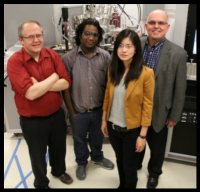
An engineering research team at the University of Alberta has invented a new transistor that could revolutionize thin-film electronic devices.
Their findings, published in the prestigious science journal Nature Communications, could open the door to the development of flexible electronic devices with applications as wide-ranging as display technology to medical imaging and renewable energy production.
The team was exploring new uses for thin film transistors (TFT), which are most commonly found in low-power, low-frequency devices like the display screen you’re reading from now. Efforts by researchers and the consumer electronics industry to improve the performance of the transistors have been slowed by the challenges of developing new materials or slowly improving existing ones for use in traditional thin film transistor architecture, known technically as the metal oxide semiconductor field effect transistor (MOSFET).
But the U of A electrical engineering team did a run-around on the problem. Instead of developing new materials, the researchers improved performance by designing a new transistor architecture that takes advantage of a bipolar action. In other words, instead of using one type of charge carrier, as most thin film transistors do, it uses electrons and the absence of electrons (referred to as “holes”) to contribute to electrical output. Their first breakthrough was forming an ‘inversion’ hole layer in a ‘wide-bandgap’ semiconductor, which has been a great challenge in the solid-state electronics field.
Once this was achieved, “we were able to construct a unique combination of semiconductor and insulating layers that allowed us to inject “holes” at the MOS interface,” said Gem Shoute, a PhD student in the Department of Electrical and Computer Engineering who is lead author on the article. Adding holes at the interface increased the chances of an electron “tunneling” across a dielectric barrier. Through this phenomenon, a type of quantum tunnelling, “we were finally able to achieve a transistor that behaves like a bipolar transistor.”
“It’s actually the best performing [TFT] device of its kind—ever,” said materials engineering professor Ken Cadien, a co-author on the paper. “This kind of device is normally limited by the non-crystalline nature of the material that they are made of”
The dimension of the device itself can be scaled with ease in order to improve performance and keep up with the need of miniaturization. An advantage that modern TFTs lack. The transistor has power-handling capabilities at least 10 times greater than commercially produced thin film transistors.
Electrical engineering professor Doug Barlage, who is Shoute’s PhD supervisor and one of the paper’s lead authors, says his group was determined to try new approaches and break new ground. He says the team knew it could produce a high-power thin film transistor—it was just a matter of finding out how.
“Our goal was to make a thin film transistor with the highest power handling and switching speed possible. Not many people want to look into that, but the raw properties of the film indicated dramatic performance increase was within reach,” he said. “The high quality sub 30 nanometre (a human hair is 50 nanometres wide) layers of materials produced by Professor Cadien’s group enabled us to successfully try these difficult concepts”
In the end, the team took advantage of the very phenomena other researchers considered roadblocks.
“Usually tunnelling current is considered a bad thing in MOSFETs and it contributes to unnecessary loss of power, which manifests as heat,” explained Shoute. “What we’ve done is build a transistor that considers tunnelling current a benefit.”
The team has filed a provisional patent on the transistor. Shoute says the next step is to put the transistor to work “in a fully flexible medium and apply these devices to areas like biomedical imaging, or renewable energy.”
Share on:


Testimonial
"Advertising in PCB007 Magazine has been a great way to showcase our bare board testers to the right audience. The I-Connect007 team makes the process smooth and professional. We’re proud to be featured in such a trusted publication."
Klaus Koziol - atgSuggested Items
AI Demand Drives PCB Material Market Growth
05/08/2026 | TPCAAs AI computing continues to drive a comprehensive upgrade in hardware specifications, the global printed circuit board industry is undergoing a profound structural transformation.
I-Connect007 Editor’s Choice: Five Must-Reads for the Week
05/01/2026 | Michelle Te, I-Connect007If it feels like the PCB industry is accelerating faster than ever, you’re not imagining it. From advanced materials driven by AI applications to renewed investment in domestic manufacturing—and the next generation stepping into critical roles—there’s a lot shifting at once. My selections for this week highlight where the pressure points are forming, and where the opportunities are emerging.
Electronics Manufacturing Needs Your Voice: Global Sentiment Survey Now Live
04/30/2026 | Global Electronics AssociationThe latest monthly Global Sentiment Survey from the Global Electronics Association is now open. At a time when demand uncertainty, policy shifts, energy costs, and supply chain recalibration are pulling the industry in multiple directions, the survey captures something macroeconomic data often misses: how manufacturers are actually experiencing conditions on the ground.
From Backbone to Breakthroughs: I-Connect007 Wraps PCB Materials Series with Focus on Innovation
05/06/2026 | I-Connect007I-Connect007 wraps up its six-part podcast series, PCB Materials: The Backbone and Future of Electronics, with Episode 6 and a discussion focusing on innovation. In Episode 6, Marcy LaRont speaks with Isola CTO Kirk Thompson about a critical turning point for the PCB industry as innovation accelerates. As data rates climb and demands from AI infrastructure, power density, flexible electronics, photonics, and chiplet integration intensify, traditional material assumptions are no longer sufficient.
Jiva Soluboard Getting the Attention It Deserves
04/30/2026 | Marcy LaRont, I-Connect007 MagazineJiva is a newer company that bridges the divide between PCB fabrication and product circularity or sustainability. Jiva Soluboard is the first fully recyclable laminate material ever created for PCB fabrication, and it's not going unnoticed. Stephen Driver, CEO of Jiva, gave us an update at APEX EXPO, including an exciting certification achievement in February.