


 Powering the Future: Why Thermal Management Defines the Future of Electronics
 Standard of Excellence: Engineering Is the New Sales—How Technical Collaboration Wins Business
 SMT Perspectives & Prospects: Artificial Intelligence, Part 7—Data Module 2


3D Assembly Processes: A Look at Today and Tomorrow
February 26, 2016 | D. Geiger, G. Thein, AEG, Flextronics International Inc.Estimated reading time: 12 minutes
Introduction
Printed circuit board assembly (PCBA), starting with the plated through-hole, later evolving to surface mount assembly, have been planar in two dimensions. Components are mounted onto the PCBA in the x and y direction, where the height, z direction, is controlled by the component height.
On the assembly level, board-to-board and board-to-flexible printed circuit (FPC) are commonly used to interconnect two or more PCBAs together to create a three-dimensional structure. On the PCB level, we will look at several techniques aimed at reducing the number of components mounted on the surface. On the PCBA level, certain 3D assembly techniques have been developed to address reduction in board available space or reduction in overall assembly thickness. These techniques include package-on-package (PoP) and cavity assembly.
We will also take a glimpse into the future, based on technologies available now, to examine potential assembly methods on the horizon for 3D assemblies.
Discussion
Assembly Level
As the PCBA started with a two-dimensional assembly using one single FR-4 rigid PCB, where plated thru hole and surface mount components are placed in the x and y direction, various methods are in use to interconnect multiple PCBAs together to create a three dimension assembly.
Board to board (B2B) level connectors are the most common. These include connectors using PTH or SMT. Some examples are daughter board mounted onto a motherboard, high speed/high density connection between backplane and functional cards, etc. B2B connections create a rigid three dimensional assembly structure where PCBA orientation has to follow the x, y, and z axis. It was difficult to interconnect PCBAs at various angles at will. PCBAs can either stack on top of each other, or be connected at 90 degrees to each other. The connector, whether PTH or SMT, also takes up valuable board surface area in today’s high density application.
Figure 1: 3D Assembly using board-to board-connectors1.
Using flexible printed circuit (FPC) as the interconnect, we can orient the PCBAs in various angles as required by the application. To connect the FPC to the rigid board, various methods have been developed. With board to FPC (B2F) connectors, the FPC can be easily inserted and removed as needed. This is most commonly used to connect the FPC from the display panel to the PCBA. To reduce the cost of the assembly by removing the connector, direct attachment method is used.
Direct attachment includes soldering, or the use of anisotropic conductive film (ACF) or paste (ACP). With soldering, it can be perform with a soldering iron, but for reliability and repeatability, typically a hot bar soldering process is used. The pads on the PCBA and FPC are pre-tinned with solder. A thermode head is designed to fit the pad areas of the FPC, and provide consistent heat to solder the FPC to the PCBA. Usually a pad-to-pad pitch of around 1.0mm is required to avoid solder bridging between pads during the hot bar soldering process. The hot bar solder joint is reworkable, but usually the FPC is damaged during removal and must be discarded, along with the display if it is attached to one. The pads on the PCBA can be cleaned up and be ready for soldering again.
To connect the FPC to the PCBA with finer pad to pad pitch (down to 0.2mm), ACF or ACP can be used. The ACF or ACP replaces the pre-tinned solder on the pads. Conductive particles inside the ACF or ACP are compressed to allow an electrical connection in the z axis between the pad on the FPC to the pad on the PCBA. Due to the pads on the FPC and PCBA which are non-solder mask defined, this creates a hill and valley profile for the ACF material. The hill (where the pads align) compresses the conductive particles. The valley (empty area) allows the conductive particles to remain in suspension in the ACF or ACP. This attachment method is reworkable, and the FPC is usually not damaged during the rework.
Figure 2: Board-to-FPC using connector.
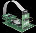
To further reduce the attachment of the FPC to the PCBA, the PCB manufacturer can now integrate the FPC as part of the rigid PCBA layer. This creates a rigid-flex PCB. This provides further flexibility on how the PCBAs on a rigid-flex can be oriented and positioned.
Figure 3: Example of a rigid-flex PCB2.
PCB Level
The top and bottom layer of a printed circuit board (PCB) are where the components are installed to form the circuitry. Physical pads and traces are needed to provide the footprint and signal path to connect the circuitry. To reduce the number of components on the top and bottom layer, while maintaining the same functionality of circuitry, buried capacitance can be used. This creates a single value of capacitance across the layers inside the PCB, usually used to replace bypass capacitors on the surface.
Figure 4: Buried capacitance inside a PCB3.
Due to miniaturization of the assembly, and the need to add more circuitry function while maintaining or reducing overall PCBA dimension, we will look at several techniques aimed at reducing the components mounted on the surface. Embedded passives place different values of resistors and capacitors inside the inner layer of PCB. Compared to buried capacitance, this allows for further reduction in components required on the top and bottom surface. Embedded actives place an integrated circuit chip into the inner layer of PCB. Both of these techniques involve assembling the components onto a single layer of PCB first, then build up multiple layers of PCB around it. Or the remaining layers are made separately and cavity is cutout to provide relief space for the embedded components.
Page 1 of 4
Share on:


Testimonial
"Our marketing partnership with I-Connect007 is already delivering. Just a day after our press release went live, we received a direct inquiry about our updated products!"
Rachael Temple - AlltematedSuggested Items
SMTA Ultra HDI Symposium, Day 2: Fragile Supply Chains, Fierce Innovation
04/14/2026 | Marcy LaRont, I-Connect007The Arizona weather yielded another beautiful day as we gathered for the second day of SMTA’s annual UHDI symposium. After the first full day discussing the role of AI in business and the how-tos of implementation, Avondale Mayor Mike Pineda kicked off day two, proud to showcase his city and to declare its important place in the continued development of the West Valley, an increasingly important area for tech and manufacturing.
KYZEN Focuses on Aqueous and Stencil Cleaning Solutions at SMTA Monterrey Expo and Tech Forum
04/10/2026 | KYZEN'KYZEN, the global leader in innovative environmentally friendly cleaning chemistries, will exhibit at the SMTA Monterrey Expo & Tech Forum.
Solder Paste Innovations for Enhanced Reliability from MacDermid Alpha Electronics Solutions
04/10/2026 | Real Time with... APEX EXPOJason Fullerton of MacDermid Alpha Electronics Solutions discusses innovative alloys like Innolot MXE, low-temperature solder options, and polymer reinforcement strategies. Learn how these solutions address the growing demands of high-performance computing and larger component assemblies, ensuring optimal performance and cost-effectiveness.
Frank Sommer Discusses Selective Soldering Innovations for EVs
04/10/2026 | Real Time with... APEX EXPODan Beaulieu sits down with Frank Sommer, a selective soldering expert from Nordson Electronics Solutions, to discuss the resurgence of selective soldering driven by electric vehicle manufacturing, and the need for robust through-hole component integration. He also introduces Nordson's innovative SELECT Synchro selective soldering machine, designed for enhanced throughput and flexibility.
Double Win: Indium Corporation’s CW-807RS and Indium12.9HF Receive EM Asia Innovation Honors
04/07/2026 | Indium CorporationIndium Corporation®, a leading materials provider for the electronics assembly market, recently received Electronics Manufacturing (EM) Asia Innovation Awards for its halogen-free CW-807RS flux-cored wire and Indium12.9HF solder paste products.