


 The Hidden Enabler of Autonomous Warfare: Advanced PCB Technologies Behind Defense AI
 Defense Speak Interpreted: Extreme Financial Disparity in Drones and Missiles
 American Made Advocacy: Five Years of Educating, Advocating, and Influencing Legislation and Policy


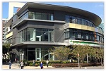
On 16th February 2016, Stadium’s Board of Directors cut the ribbon to signify the official opening ceremony for its Regional Design Centre (RDC) in Shanghai’s Zhangjiang Hi-Tech Park, China.
In support of the Group’s wider strategy to further develop its design-led technology businesses, the Shanghai RDC has become an International Purchasing Office (IPO) and the Company’s regional research and development hub in wireless M2M connectivity for global OEM products in automotive, medical, security and other growing vertical markets. Driven by the Internet of Things (IoT), which continues to stimulate demand, the M2M space is forecast for high growth.
“The new Shanghai Regional Design Centre is an exciting move for Stadium that both strengthens our wireless capabilities and gives us access into new markets,” said Charlie Peppiatt, CEO, Stadium Group. “We have recruited a highly experienced team, including design engineers and field application engineers, specialising in wireless, RF and M2M technologies. Stadium’s presence in China, delivered by the new Shanghai RDC and manufacturing facility in Dongguan, positions the company to capitalise on a growing market opportunity and expand further into the Asia Pacific market.”
A 210 m² site on the Zhangjiang Hi-Tech Park was selected as the location for Stadium’s RDC office. Located on the Pudong side of the city, this high-tech park is host to a large number of industries including integrated circuits, software, IoT development, biopharmaceuticals, information security, semiconductor illumination and modern agriculture, among others. A significant number of multinationals also have their research and development centres located here. The talent pool in Zhangjiang Hi-Tech Park for electronics engineering and related skills is the best in Asia with a vast pool of experienced skilled doctorates and graduates.


