


 Dan’s Biz Bookshelf: Four Important Books You Need to Read (Not Just Say You Have)
 The Marketing Minute: Cracking the Code of Technical Marketing


Graphene Nanoribbons: It's All about the Edges
March 24, 2016 | EMPAEstimated reading time: 3 minutes
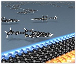
As electronic components are becoming ever smaller, the industry is gradually approaching the limits of what is achievable using the traditional approach with silicon as a semiconductor material. Graphene, the material with a number of "miraculous" properties, is considered a possible replacement. The one atom thin carbon film is ultra-light, extremely flexible and highly conductive. However, in order to be able to use graphene for electronic components such as field effect transistors, the material has to be "transformed" into a semiconductor. This was achieved by Empa scientists some time ago using a newly developed method - in 2010, they presented, for the first time, graphene nanoribbons (GNR) only a few nanometres wide with precisely shaped edges. For this, the ribbons were grown on a metal surface from specifically designed precursor molecules. The narrower the ribbons, the larger their electronic band gap - i.e. the energy range in which no electrons can be located, which is responsible for ensuring that an electronic switch (for example, a transistor) can be turned on and off. The Empa researchers were then also able to "dope" the nanoribbons, i.e. to furnish the ribbons with impurity atoms such as nitrogen at certain points, in order to influence the electronic properties of the graphene ribbons even more.
The perfect blueprint
In the paper now published in Nature, the Empa team led by Roman Fasel reports, together with colleagues from the Max Planck Institute for Polymer Research in Mainz, headed by Klaus Müllen, and from the Technical University of Dresden led by Xinliang Feng, how it managed to synthesise GNR with perfectly zigzagged edges using suitable carbon precursor molecules and a perfected manufacturing process. The zigzags followed a very specific geometry along the longitudinal axis of the ribbons. This is an important step, because researchers can thus give graphene ribbons different properties via the geometry of the ribbons and especially via the structure of their edges.
As with floor tiling, the right tiles - or precursor molecules - for the synthesis on the surface first had to be found for the specific pattern of the zigzag graphene ribbons. Unlike in organic chemistry, which takes the occurrence of by-products into account on the path to achieving a pure substance, everything had to be designed for the surface synthesis of the graphene ribbons so that only a single product was produced. The scientists repeatedly switched back and forth between computer simulations and experiments, in order to design the best possible synthesis. With molecules in a U-shape, which they allowed to grow together to form a snake-like shape, and additional methyl groups, which completed the zigzag edges, the researchers were able to finally create a "blueprint" for GNR with perfect zigzag edges. To check that the zigzag edges were exact down to the atom, the researchers investigated the atomic structure using an atomic force microscope (AFM). In addition, they were able to characterise the electronic states of the zigzag edges using scanning tunnelling spectroscopy (STS).
Page 1 of 2
Share on:


Testimonial
"The I-Connect007 team is outstanding—kind, responsive, and a true marketing partner. Their design team created fresh, eye-catching ads, and their editorial support polished our content to let our brand shine. Thank you all! "
Sweeney Ng - CEE PCBSuggested Items
Aismalibar North America Showcases Advanced Thermal Management Solutions at The Battery Show North America 2025
09/18/2025 | AismalibarAismalibar North America, a leader in high-performance thermal management solutions, will present its latest innovations at The Battery Show North America and Electric & Hybrid Vehicle Technology Expo 2025 in Detroit, Michigan, October 6–9, 2025, where attendees can meet the team at Booth #5929 to explore materials engineered for demanding EV and high-power electronics.
Electrodeposited Copper Foils Market to Grow by $11.7 Billion Over 2025-2032
09/18/2025 | Globe NewswireThe global electrodeposited copper foils market is poised for dynamic growth, driven by the rising adoption in advanced electronics and renewable energy storage solutions.
Breakthrough in Non-Contact Solder Removal Earns Kurtz Ersa 2025 Mexico Technology Award at SMTA Guadalajara
09/18/2025 | Kurtz Ersa Inc.Kurtz Ersa Inc., a leading supplier of electronics production equipment, is proud to announce that it has been awarded a 2025 Mexico Technology Award in the category of Rework & Repair for its HR 600P Automatic Rework System.
A.R.T. Invests in Latest Equipment to Further Enhance Electronics Training Facilities
09/17/2025 | A.R.T. Ltd.Advanced Rework Technology Ltd. (A.R.T.), a leading independent IPC-accredited training provider, has announced a series of new equipment investments at its state-of-the-art training centre.
Richardson Electronics Appoints Daniel Albers to Drive Made-in-USA Contract Manufacturing Expansion
09/17/2025 | Globe NewswireRichardson Electronics, Ltd., a global provider of engineered solutions for the green energy, power management, and custom display markets, announced the appointment of Daniel Albers to spearhead business development for its expanded, Made-in-USA contract manufacturing efforts.