


 Dan’s Biz Bookshelf: ‘Atomic Habits’
 Happy’s Tech Talk #48: Digital Twins—Integrating Design and Manufacturing
 The Chemical Connection: The Consequences of Additive Metallizing on Etching Steps


Delighted to be invited to an exclusive preview of the new PhiChem global headquarters and R&D centre in Shanghai’s Baoshan suburb, I joined the VIP group assembled at the PhiChem booth at the CPCA show, made welcome by PhiChem President Dr. Jin Zhang.
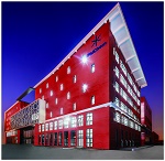
An hour’s private bus ride brought us to an immaculately presented site—four brand-new buildings with a total of 500,000 square feet of floor area: administration, pilot plant manufacturing and packaging, warehousing, fronted by a spectacularly impressive six-story laboratory complex, which had taken five years from green-field site to completion.
Gleaming! Through reception and into a display area with glass showcases holding examples of PhiChem’s products and applications, and an appropriate place for Dr. Zhang to begin his explanation of PhiChem’s evolution since he founded the company in 2002.
A graduate chemist, with an MS degree in optics, and many years’ experience in microelectronics packaging and the development of optical and laser materials and components, Jin Zhang gained his doctorate in polymer chemistry at the University of Michigan in the U.S. Recognising the rapid growth in the demand for optical fibres for data and telecoms transmission, and a fundamental requirement for glass fibres to be coated for mechanical protection and enhancement of their optical properties, Dr. Zhang returned to China and began production of UV-curable coating resins in Shanghai. Since 2002, PhiChem has grown to become China’s largest supplier of UV-curable materials to the optical fibre industry and second largest in the world, producing all of its own raw materials and resin precursors.
Dr. Zhang reached into a display cabinet and took a short length of fibre from a large spool, explaining that the widespread use of high bandwidth optical fibre would not have been feasible without the protection afforded by UV-curable coatings. The sample he demonstrated had a coated diameter of 250 microns, the glass itself being half that diameter, and the combination of glass and coating had a tensile strength of five kilograms. Talking of high speed, he remarked that the fibre was coated and cured on-the-fly at 3000 metres per minute!
Page 1 of 3


