


 Dan’s Biz Bookshelf: Four Important Books You Need to Read (Not Just Say You Have)
 The Marketing Minute: Cracking the Code of Technical Marketing


Terahertz Technology Reaches Industrial Maturity
April 6, 2016 | Fraunhofer IBMTEstimated reading time: 4 minutes
Terahertz is a new technology in which nondestructive testing of components and surfaces is possible. Until now, these devices and, in particular, the sensor heads have been expensive and unwieldy. Researchers at Fraunhofer have now succeeded in making sensor heads more compact and, thus, cheaper, which facilitates their handling considerably. First prototypes are already being used for the production of plastic pipes. They are also very well suited for analyzing coatings of fiber composites. From April 25 to 29, 2016, these new sensor heads are being presented at the Hannover Messe (Hall 2, Stand C16/C22).
More than ten years ago, terahertz technology was the next big thing. Back then there was a lot of talk about ‚nude‘ body scanners. People thought that the devices that were being installed at airports were going to make revealing images of passengers. Moreover, scientists were hoping to develop measurement systems for material testing and inspection of components using terahertz radiation. Despite all these great expectations, the long-awaited breakthrough for terahertz technology did not come about. Compared to the conventional methods currently used for non-destructive testing, such as X-ray or ultrasound, terahertz technology is simply too expensive, unwieldy and overall impractical.
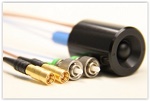
Measuring system with the innovative sensor head
The latest developments of the Fraunhofer Institute for Telecommunication, Heinrich Hertz Institut, HHI in Berlin, could now give terahertz technology a decisive boost. The research team of Thorsten Göbel, who heads the Terahertz Research Group at HHI, has succeeded in developing terahertz devices that for the first time are made from standard and therefore low-cost components and are also relatively easy to handle. At the Hannover Messe, the experts will be presenting a terahertz measuring system with an innovative sensor head, which allows easy testing of various components, such as plastic tubes. The principle employed by Fraunhofer HHI for generating terahertz radiation is based on an optoelectronic method. Using a special semiconductor, laser light pulses are converted into electrical terahertz pulses that are only one billionth of a second long.
The reason for the lack of success of the terahertz technology until now is mainly due to the required properties of the semiconductors being used. These could only be achieved with materials that required an illumination with a wavelength of 800 nanometers. Both the terahertz system‘s laser and optical components are too expensive and not robust enough for industrial use when using this rather exotic wavelength.
Page 1 of 2
Share on:


Testimonial
"The I-Connect007 team is outstanding—kind, responsive, and a true marketing partner. Their design team created fresh, eye-catching ads, and their editorial support polished our content to let our brand shine. Thank you all! "
Sweeney Ng - CEE PCBSuggested Items
Indium Corporation Earns Mexico Technology Award for New Halogen-Free Flux-Cored Wire
09/18/2025 | Indium CorporationIndium Corporation recently earned a Mexico Technology Award for its new high-reliability, halide- and halogen-free flux-cored wire, CW-807RS, which improves wetting speeds and cycle times for electronics assembly and robot soldering applications.
Blaize, Technology Control Company Partner to Power Saudi Arabia’s Next-Generation AI Innovation Infrastructure
09/17/2025 | BUSINESS WIREBlaize Holdings, Inc., a leader in programmable, energy-efficient edge AI computing, and Technology Control Company (TCC), a leading technology solutions provider in the Kingdom of Saudi Arabia (KSA), announced a strategic partnership to advance Saudi Arabia’s AI innovation infrastructure and accelerate its digital transformation goals.
BLT Joins Microchip Partner Program as Design Partner
09/17/2025 | BUSINESS WIREBLT, a U.S.-owned and operated engineering design services firm announced it has joined the Microchip Design Partner Program.
Curing and Verification in PCB Shadow Areas
09/17/2025 | Doug Katze, DymaxDesign engineers know a simple truth that often complicates electronics manufacturing: Light doesn’t go around corners. In densely populated PCBs, adhesives and coatings often fail to fully cure in shadowed regions created by tall ICs, connectors, relays, and tight housings.
On the Line With… Podcast: UHDI and RF Performance
09/17/2025 | I-Connect007I-Connect007 is excited to announce the release of a new episode in its latest On the Line with... podcast series, which shines a spotlight on one of the most important emerging innovations in electronics manufacturing: Ultra-High-Density Interconnect (UHDI).