


 Dan’s Biz Bookshelf: Four Important Books You Need to Read (Not Just Say You Have)
 The Marketing Minute: Cracking the Code of Technical Marketing


Physicists Develop a Cooling System for the Processors of the Future
April 20, 2016 | ACSEstimated reading time: 3 minutes
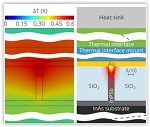
Researchers from MIPT have found a solution to the problem of overheating of active plasmonic components. These components will be essential for high-speed data transfer within the optoelectronic microprocessors of the future, which will be able to function tens of thousands of times faster than the microprocessors currently in use today. In the paper published in ACS Photonics the researchers have demonstrated how to efficiently cool optoelectronic chips using industry-standard heatsinks in spite of high heat generation in active plasmonic components.
The speed of multicore and manycore microprocessors, which are already used in high-performance computer systems, depends not so much on the speed of an individual core, but rather on the time it takes for data to be transferred between the cores. The electrical copper interconnects used in microprocessors today are fundamentally limited in bandwidth, and they cannot be used to maintain the continuing growth of the processor performance. In other words, doubling the number of cores will not double the processing power.
Leading companies in the semiconductor industry, such as IBM, Oracle, Intel, and HP, see the only solution to this problem in switching from electronics to photonics, and they are currently investing billions of dollars into this. Replacing electrons with photons will mean that large amounts of data will be able to be transferred between processor cores almost instantly, which in turn will mean that the processor performance will be nearly proportional to the number of cores. However, due to diffraction, photonic components are not as easy to scale down as electronic components. Their dimensions cannot be smaller than the size approximately equal to the light wavelength (~ 1 micrometer or 1000 nanometers), but transistors will soon be as small as 10 nanometers. This fundamental problem can be solved by switching from bulk waves to surface waves, which are known as surface plasmon polaritons (SPPs). This will enable to confine light on the nanoscale. Along with the leading research centers of industrial companies and the laboratories of leading universities, Russian scientists from the Laboratory of Nanooptics and Plasmonics of MIPT’s Center of Nanoscale Optoelectronics are also making good progress in this field.
Page 1 of 2
Share on:


Testimonial
"The I-Connect007 team is outstanding—kind, responsive, and a true marketing partner. Their design team created fresh, eye-catching ads, and their editorial support polished our content to let our brand shine. Thank you all! "
Sweeney Ng - CEE PCBSuggested Items
Electrodeposited Copper Foils Market to Grow by $11.7 Billion Over 2025-2032
09/18/2025 | Globe NewswireThe global electrodeposited copper foils market is poised for dynamic growth, driven by the rising adoption in advanced electronics and renewable energy storage solutions.
MacDermid Alpha Showcases Advanced Interconnect Solutions at PCIM Asia 2025
09/18/2025 | MacDermid Alpha Electronics SolutionsMacDermid Alpha Electronic Solutions, a global leader in materials for power electronics and semiconductor assembly, will showcase its latest interconnect innovations in electronic interconnect materials at PCIM Asia 2025, held from September 24 to 26 at the Shanghai New International Expo Centre, Booth N5-E30
Trouble in Your Tank: Implementing Direct Metallization in Advanced Substrate Packaging
09/15/2025 | Michael Carano -- Column: Trouble in Your TankDirect metallization systems based on conductive graphite are gaining popularity throughout the world. The environmental and productivity gains achievable with this process are outstanding. Direct metallization reduces the costs of compliance, waste treatment, and legal issues related to chemical exposure. A graphite-based direct plate system has been devised to address these needs.
Closing the Loop on PCB Etching Waste
09/09/2025 | Shawn Stone, IECAs the PCB industry continues its push toward greener, more cost-efficient operations, Sigma Engineering’s Mecer System offers a comprehensive solution to two of the industry’s most persistent pain points: etchant consumption and rinse water waste. Designed as a modular, fully automated platform, the Mecer System regenerates spent copper etchants—both alkaline and acidic—and simultaneously recycles rinse water, transforming a traditionally linear chemical process into a closed-loop system.
Driving Innovation: Depth Routing Processes—Achieving Unparalleled Precision in Complex PCBs
09/08/2025 | Kurt Palmer -- Column: Driving InnovationIn PCB manufacturing, the demand for increasingly complex and miniaturized designs continually pushes the boundaries of traditional fabrication methods, including depth routing. Success in these applications demands not only on robust machinery but also sophisticated control functions. PCB manufacturers rely on advanced machine features and process methodologies to meet their precise depth routing goals. Here, I’ll explore some crucial functions that empower manufacturers to master complex depth routing challenges.