


 Dan’s Biz Bookshelf: Four Important Books You Need to Read (Not Just Say You Have)
 The Marketing Minute: Cracking the Code of Technical Marketing


NRL Reveals Novel Uniform Coating Process of p-ALD
April 21, 2016 | NRLEstimated reading time: 3 minutes
Scientists at the U.S. Naval Research Laboratory (NRL) have devised a clever combination of materials - when used during the thin-film growth process - to reveal that particle atomic layer deposition, or p-ALD, deposits a uniform nanometer-thick shell on core particles regardless of core size, a discovery having significant impacts for many applications since most large scale powder production techniques form powder batches that are made up of a range of particles sizes.
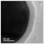
Image shows high magnification bright field transmission electron microscopy (TEM) image showing obvious delineation of alumina film and surface of particle. In this work, performed by NRL researchers, the growth per cycle (GPC) during atomic layer deposition is compared for different batches of powder with average particle sizes ranging from nanometer (nm) to micrometer (μm). Samples prepared after depositing thin alumina films (from 10 to15 nm) on tungsten powders using particle atomic layer deposition (p-ALD) were investigated with x-ray photoelectron spectroscopy (XPS), scanning and transmission electron microscopy (SEM), and TEM.
(U.S. Naval Research Laboratory)
"Particle atomic layer deposition is highlighted as a technology that can create new and exciting designer core/shell particles to be used as building blocks for the next generation of complex multifunctional nanocomposites," said Dr. Boris Feygelson, research engineer, NRL Electronics Science and Technology Division. "Our work is important because shell-thickness is most often a crucial parameter in applications where core-shell materials can be used to enhance performance of future materials."
Atomic layer deposition is a layer-by-layer chemical vapor deposition-based thin-film growth technique used extensively in the electronics industry to deposit nanometer-thick films of dielectric materials on devices. Combined with other deposition and shadowing masking techniques, ALD is an integral part of electronic chip and device manufacturing. The same gas-phase process can be applied in a rotary or fluidizing powder bed reactor to grow nanometer-thick films that are highly conformal and uniformly thick on individual particles.
Previous research on p-ALD, patented by ALD NanoSolutions, Inc., has shown that growth of each layer during the deposition process varies with particle size, with the underlying assumption that larger particles will always have less growth. To observe this growth phenomenon, the NRL team grew alumina on nano- and micron-sized particles of tungsten and measured the shell thickness in a transmission electron microscope. Because of the huge mass/density difference of the two materials, this pairing provides maximum contrast in the electron microscope and delineation was easily distinguishable between the particle core and shell.
In their research, the scientists created core and shell powders consisting of a tungsten particle core and thin alumina shell that were then synthesized using atomic layer deposition in a rotary reactor. Standard atomic layer deposition of trimethylaluminum and water was performed on varying batches of powder with different average particle sizes.
"Amazingly, we found that the growth per cycle of the alumina film on an individual particle in a batch was shown to be independent of the size of an individual particle, and therefore, a powder batch - which consists of particles sizes spanning orders of magnitude - has constant shell thicknesses on all particles. This result upsets the current understanding of ALD on particles," said Dr. Kedar Manandhar, ASEE postdoc, NRL Electronics Science and Technology Division and leading author of the research paper.
The work, published recently in the Journal of Vacuum Science and Technology A, suggests that water, a reactant in the ALD process, is reason for the same rate of growth on different particles. This uniformity of thickness on different particle sizes in a particular batch is determined to be due to the difficulty of removing residual water molecules from the powder during the purging cycle of the atomic layer deposition (ALD) process. "Water is very sticky and it is very difficult to remove the last mono-layer from surfaces," Feygelson says. "And when you have a tumbling bed of powders, the water sticks around between the particles and results in consistent shell growth in the tumbling powder.
Applications for this research demonstrate implications for use in materials like abrasion resistant paints, high surface area catalyst, electron tunneling barriers, ultra-violet adsorption or capture in sunscreens or solar cells and even beyond when core-shell nanoparticles are used as buildings blocks for making new artificial nanostructured solids with unprecedented properties.
This research is a cross-disciplinary effort at NRL between the Materials Science and Technology Division and Electronics Science and Technology Division. The authors of the paper gratefully acknowledge Drs. Dev Palmer (Defense Advanced Research Projects Agency), Baruch Levush (NRL), and Fritz Kub (NRL).
Share on:


Testimonial
"Advertising in PCB007 Magazine has been a great way to showcase our bare board testers to the right audience. The I-Connect007 team makes the process smooth and professional. We’re proud to be featured in such a trusted publication."
Klaus Koziol - atgSuggested Items
PC Graphics Add-in Board Shipments Up 27% QoQ in 2Q25
09/03/2025 | Jon Peddie ResearchAccording to a new research report from the analyst firm Jon Peddie Research, the growth of the global PC-based graphics add-in board market reached 11.6 million units in Q2'25 and desktop PC CPUs shipments increased to 21.7 million units.
PC GPU Shipments Up 8.4% in 2Q25 on Pre-Tariff Demand
09/02/2025 | Jon Peddie ResearchJon Peddie Research reports the growth of the global PC-based graphics processor unit (GPU) market reached 74.7 million units in Q2'25, and PC CPU shipments increased to 66.9 million units.
20 Years of Center Nanoelectronic Technologies (CNT) – Backbone of German Semiconductor Research Celebrates Anniversary
08/14/2025 | Fraunhofer IPMSThe Center Nanoelectronic Technologies (CNT) of the Fraunhofer Institute for Photonic Microsystems (IPMS) is celebrating its 20th anniversary this year. Since its founding in 2005, it has developed into a pillar of applied semiconductor research in Germany and Europe. With its unique research cleanroom and equipment adhering to the 300-mm wafer industry standard, CNT is unparalleled in Germany and serves as a central innovation driver for the microelectronics industry.
Q2 Client CPU Shipments Increased 8% from Last Quarter, Up 13% YoY
08/13/2025 | Jon Peddie ResearchJon Peddie Research reports that the global client CPU market expanded for two quarters in a row, and in Q2’25, it showed unseasonal growth of 7.9% from last quarter, while server CPU shipments increased 22% year over year.
FuriosaAI Closes $125M Investment Round to Scale Production of Next-Gen AI Inference Chip
07/31/2025 | BUSINESS WIREFuriosaAI, a semiconductor company building a new foundation for AI compute, today announced it has completed a $125 million Series C bridge funding round. The investment continues a period of significant momentum for Furiosa as global demand for high-performance, efficient AI infrastructure soars.