


 American Made Advocacy: Smart Policies Can Ensure AI Data Centers Are Secure
 Beyond the Board: Early Engagement Means Faster Prototyping for Defense Programs
 Defense Speak Interpreted: The Autonomous Plane Battle—Skyborg Vs. Loyal Wingman


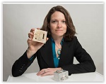
NASA Investigates 3-D Printing for Building Densely Populated Electronic Assemblies
April 26, 2016 | NASAEstimated reading time: 2 minutes
As detector assemblies get smaller and denser — packed with electronic components that all must be electrically connected to sense and read out signals — it’s becoming increasingly more challenging to design and manufacture these all-important instrument devices.
A team of NASA technologists at the Goddard Space Flight Center in Greenbelt, Maryland, however, has begun investigating the use of a technique called aerosol jet printing or direct-write manufacturing to produce new detector assemblies that are not possible with traditional assembly processes.
“If we succeed, aerosol jet technology could define a whole new way to create dense electronic board assemblies and potentially improve the performance and consistency of electronic assemblies,” explained Goddard technologist Beth Paquette, who is leading the R&D effort that began last fiscal year. Furthermore, aerosol jet printing promises to slash the time it takes to manufacture circuit boards, from a month to a day or two, she added.
Important Distinction
As with other 3-D printing techniques, aerosol jet manufacturing builds components by depositing materials layer-by-layer following a computer-aided design, or CAD, drawing. However, jet aerosol printing offers an important difference.
Instead of melting and fusing plastic powder or some other material in precise locations, as in the case of many 3-D printers, aerosol jet printing uses a carrier gas and printer heads to deposit a fine aerosol of metal particles, including silver, gold, platinum, or aluminum, onto a surface. Aerosol jet printers also can deposit polymers or other insulators and can even print carbon nanotubes, cylindrically shaped carbon molecules that have novel properties useful in nanotechnology, electronics, and optics.
“It can print around bends, on spheres or on something flat, or on a flexible surface, which then can be flexed into the shape you want,” she said.
These attributes make the technology ideal for detector assemblies, particularly those that need to be shaped differently or are very small, yet dense because of the large number of tiny components that must be electrically wired or linked together on a circuit board — an inescapable reality as instruments get smaller and smaller.
“We can make these wires microns in width,” Paquette said. “These lines are very small, down to 10 microns wide. These sizes aren’t possible using traditional circuit board manufacturing processes.” (By way of comparison, the average human hair measures between 17 and 191 microns in width.)
Page 1 of 2
Share on:


Testimonial
"Your magazines are a great platform for people to exchange knowledge. Thank you for the work that you do."
Simon Khesin - Schmoll MaschinenSuggested Items
High Density Packaging User Group Announces ASKPCB Membership
11/03/2025 | HDP User GroupHigh Density Packaging User Group (HDP) is pleased to announce that the Aoshikang Technology (Hong Kong) Co., Ltd (ASKPCB) has become a member.
Cephia Secures $4M Seed Funding to Revolutionize Multimodal Sensing with Metasurface Technology
10/31/2025 | PRNewswireCephia, a startup building products using advanced AI computational imaging technologies and silicon sensors made from advanced metamaterials, formally launched with several pilot customers and $4 million in seed venture capital funding.
KYZEN Honored with 2025 Step-by-Step Excellence Award for Its Innovative ANALYST² Process Control System
10/31/2025 | KYZEN'KYZEN, the global leader in innovative environmentally responsible cleaning chemistries, is proud to announce that its ANALYST² Process Control System has won a 2025 Step-by-Step Excellence Award (SbSEA).
LPKF Delivers Key Strategic Technology to Fraunhofer's Glass Panel Technology Group
10/29/2025 | LPKFLPKF Laser & Electronics SE is one of the initiators of the Glass Panel Technology Group (GPTG), a consortium encompassing the entire process chain for advanced semiconductor packaging with glass substrates.
On the Line With… Ultra HDI Podcast—Episode 7: “Solder Mask: Beyond the Traces,” Now Available
10/31/2025 | I-Connect007I-Connect007 is excited to announce the release of the seventh episode of its 12-part podcast series, On the Line With… American Standard Circuits: Ultra HDI. In this episode, “Solder Mask: Beyond the Traces,” host Nolan Johnson sits down with John Johnson, Director of Quality and Advanced Technology at American Standard Circuits, to explore the essential role that solder mask plays in the Ultra HDI (UHDI) manufacturing process.