


 Dan’s Biz Bookshelf: ‘Elevate: Push Beyond Your Limits'
 The Marketing Minute: The First Step to More Sales—Marketing
 It’s Only Common Sense: Customer Service Is Sales in Disguise


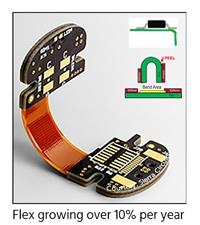
New Cadence Allegro Enhances Flex and Rigid-Flex Capabilities
May 4, 2016 | Cadence Design Systems, Inc.Estimated reading time: 3 minutes
Cadence Design Systems has unveiled the Allegro 17.2-2016 portfolio, which enables a more predictable and shorter design cycle. The portfolio features comprehensive in-design inter-layer checking technology that minimizes design-check-redesign iterations and a new dynamic concurrent team design capability that accelerates product creation time by up to 50 percent. Utilizing material inlay fabrication techniques, these new capabilities can reduce material costs by up to 25 percent. In addition, embedded Sigrity technology now ensures critical signals meet performance criteria and power integrity (PI) for PCB designers addressing power delivery and IR-drop issues efficiently, eliminating time-consuming iterations with PI experts.
The Allegro portfolio includes key advancements that minimize design iterations and lower overall cost for flex and rigid-flex designs commonly used in automotive, consumer electronics, computing, communications, mobile and wearable applications. These capabilities include:
- Rigid-Flex design enhancements that give designers the ability to specify multiple rigid and flex stack-ups in the same database. This stack-up-by-zone feature can also be used in rigid designs to create material inlay regions leveraging a mix of expensive and inexpensive materials, enabling reduction of material cost by up to 25 percent.
- Unique and comprehensive in-design inter-layer checks for flex and rigid-flex that saves manual effort and ensures all rules for advance flex designs are adhered to, avoiding many design-check-redesign iterations.
- PI for PCB designers that leverages Allegro and Sigrity technologies to provide faster, more reliable access to IR-drop analysis results, enabling PCB designers to efficiently meet power delivery network (PDN) design requirements.
- Interoperable Allegro and Sigrity technologies that provide an easy to use environment, which shortens design and verification time. This is achieved by avoiding unnecessary physical prototype iterations through improved route channel utilization using tabbed routing, new in-design backdrilling rules and efficient sharing of custom return path via structures optimized with Sigrity technology.
- New Native 3D engine that streamlines the system design process and provides improved visualization and collision detection to avoid unnecessary MCAD/ECAD iterations.
The Allegro portfolio now provides synchronous team design capability, which can shorten design time by up to 50 percent for dense designs and increase efficiency by enabling the team to design synchronously. This feature enables PCB designers to achieve maximum productivity by allowing up to five PCB designers to conduct real-time, concurrent PCB design work within the same design database, shortening time to route a dense design by up to 80 percent.
"Due to the nature of our business, flex designs are extremely critical to many of our products, specifically in the mobile and automotive space. The breadth and the depth of enhancements have the ability to significantly improve our PCB design productivity in designing for space-constrained applications," said Greg Bodi, director of System Engineering PCB Layout, Nvidia. "The new inter-layer check capability provides comprehensive in-design, real-time checks, which will save us significant time currently spent doing manual checks after layout is completed on advance flex and rigid-flex designs."
"The latest Allegro release provides many productivity and ease of use improvements," said Dave Elder, PCB Engineering manager at Tait Communications. "In-design inter-layer checks for flex and rigid-flex design is comprehensive and extensible, which can save us 20 to 25 percent time for rigid-flex designs. This will also allow us to retire some homegrown solutions we put in place."
"The new Allegro platform addresses many challenges faced by PCB designers on a daily basis," said Saugat Sen, vice president of R&D, PCB and IC Packaging Group at Cadence. "We continue to provide market-leading solutions with Allegro's extensive Rigid/Flex capabilities coupled with industry-leading power aware Sigrity SI/PI technology to reduce design cycle time for our customers' compact, high-performance products."
About Cadence
Cadence enables global electronic design innovation and plays an essential role in the creation of today's integrated circuits and electronics. Customers use Cadence software, hardware, IP and services to design and verify advanced semiconductors, consumer electronics, networking and telecommunications equipment, and computer systems. The company is headquartered in San Jose, Calif., with sales offices, design centers and research facilities around the world to serve the global electronics industry. More information about the company, its products and its services is available at www.cadence.com.
Share on:


Suggested Items
ESD Alliance Reports Electronic System Design Industry Posts $5.1 Billion in Revenue in Q1 2025
07/16/2025 | SEMIElectronic System Design (ESD) industry revenue increased 12.8% to $5,098.3 million in the first quarter of 2025 from the $4,521.6 million registered in the first quarter of 2024, the ESD Alliance, a SEMI Technology Community, announced in its latest Electronic Design Market Data (EDMD) report.
Beyond Design: Refining Design Constraints
07/17/2025 | Barry Olney -- Column: Beyond DesignBefore starting any project, it is crucial to develop a thorough plan that encompasses all essential requirements. This ensures that the final product not only aligns with the design concept but is also manufacturable, reliable, and meets performance expectations. High-speed PCB design requires us to not only push technological boundaries but also consider various factors related to higher frequencies, faster transition times, and increased bandwidths during the design process.
Prague PEDC: Call for Abstracts Deadline July 31
07/16/2025 | Pan-European Electronics Design Conference (PEDC)The second Pan-European Electronics Design Conference (PEDC) will take place Jan. 21-22, 2026, in Prague, Czech Republic. The call for abstracts deadline is July 31. Organized jointly by the German Electronics Design and Manufacturing Association (FED) and the Global Electronics Association PEDC serves as a European platform for knowledge exchange, networking, and innovation in electronics design and development.
The Pulse: Design Constraints for the Next Generation
07/16/2025 | Martyn Gaudion -- Column: The PulseIn Europe, where engineering careers were once seen as unpopular and lacking street credibility, we have been witnessing a turnaround in the past few years. The industry is now welcoming a new cohort of designers and engineers as people are showing a newfound interest in the profession.
Flexible Circuit Technologies Welcomes Regional Business Development Manager Derek Rossberg
07/15/2025 | Flexible Circuit TechnologiesFlexible Circuit Technologies a Minnesota-based flexible circuit and advanced electronics contract manufacturer, welcomes Derek Rossberg as Regional Business Development Manager.