


 Dan’s Biz Bookshelf: Four Important Books You Need to Read (Not Just Say You Have)
 The Marketing Minute: Cracking the Code of Technical Marketing


Under Pressure: New Technique Could Make Large, Flexible Solar Panels More Feasible
May 17, 2016 | Pennsylvania State UniversityEstimated reading time: 1 minute
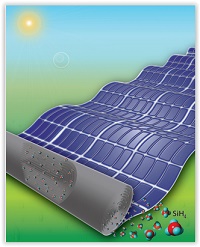
A new, high-pressure technique may allow the production of huge sheets of thin-film silicon semiconductors at low temperatures in simple reactors at a fraction of the size and cost of current technology. A paper describing the research by scientists at Penn State University publishes on May 13, 2016, in the journal Advanced Materials.
"We have developed a new, high-pressure, plasma-free approach to creating large-area, thin-film semiconductors," said John Badding, professor of chemistry, physics, and materials science and engineering at Penn State and the leader of the research team. "By putting the process under high pressure, our new technique could make it less expensive and easier to create the large, flexible semiconductors that are used in flat-panel monitors and solar cells and are the second most commercially important semiconductors."
Thin-film silicon semiconductors typically are made by the process of chemical vapor deposition, in which silane -- a gas composed of silicon and hydrogen -- undergoes a chemical reaction to deposit the silicon and hydrogen atoms in a thin layer to coat a surface. To create a functioning semiconductor, the chemical reaction that deposits the silicon onto the surface must happen at a low enough temperature so that the hydrogen atoms are incorporated into the coating rather than being driven off like steam from boiling water. With current technology, this low temperature is achieved by creating plasma -- a state of matter similar to a gas made up of ions and free electrons -- in a large volume of gas at low pressure. Massive and expensive reactors so large that they are difficult to ship by air are needed to generate the plasma and to accommodate the large volume of gas required.
"With our new high-pressure chemistry technique, we can create low-temperature reactions in much smaller spaces and with a much smaller volume of gas," said Badding. "The reduced space necessary allows us, for the first time, to create semiconductors on multiple, stacked surfaces simultaneously, rather than on just a single surface. To maximize the surface area, rolled-up flexible surfaces can be used in a very simple and far more compact reactor. The area of the resulting rolled-up semiconducting material could, upon further development, approach or even exceed a square kilometer."
Share on:


Testimonial
"In a year when every marketing dollar mattered, I chose to keep I-Connect007 in our 2025 plan. Their commitment to high-quality, insightful content aligns with Koh Young’s values and helps readers navigate a changing industry. "
Brent Fischthal - Koh YoungSuggested Items
Driving Innovation: Depth Routing Processes—Achieving Unparalleled Precision in Complex PCBs
09/08/2025 | Kurt Palmer -- Column: Driving InnovationIn PCB manufacturing, the demand for increasingly complex and miniaturized designs continually pushes the boundaries of traditional fabrication methods, including depth routing. Success in these applications demands not only on robust machinery but also sophisticated control functions. PCB manufacturers rely on advanced machine features and process methodologies to meet their precise depth routing goals. Here, I’ll explore some crucial functions that empower manufacturers to master complex depth routing challenges.
Polar Instruments Announces Additive Transmission Line Support for Si9000e
08/20/2025 | Polar InstrumentsTransmission lines embedded into the PCB surface are a feature of UHDI constructions. The 2025 fall release of Polar's Si9000e PCB impedance & insertion loss transmission line field solver incorporates eight new single ended, differential and coplanar transmission line structures.
Henniker Plasma Launches Stratus Turnkey Plasma Manufacturing Cell
08/13/2025 | Henniker PlasmaHenniker Plasma, a leading manufacturer of plasma treatment systems, proudly announces the launch of its Stratus Plasma Manufacturing Cell range — a fully integrated, turnkey solution that combines advanced atmospheric plasma surface treatment with robotic automation.
Trouble in Your Tank: Metallizing Flexible Circuit Materials—Mitigating Deposit Stress
08/04/2025 | Michael Carano -- Column: Trouble in Your TankMetallizing materials, such as polyimide used for flexible circuitry and high-reliability multilayer printed wiring boards, provide a significant challenge for process engineers. Conventional electroless copper systems often require pre-treatments with hazardous chemicals or have a small process window to achieve uniform coverage without blistering. It all boils down to enhancing the adhesion of the thin film of electroless copper to these smooth surfaces.
Designers Notebook: Basic PCB Planning Criteria—Establishing Design Constraints
07/22/2025 | Vern Solberg -- Column: Designer's NotebookPrinted circuit board development flows more smoothly when all critical issues are predefined and understood from the start. As a basic planning strategy, the designer must first consider the product performance criteria, then determine the specific industry standards or specifications that the product must meet. Planning also includes a review of all significant issues that may affect the product’s manufacture, performance, reliability, overall quality, and safety.