


 Dan’s Biz Bookshelf: Four Important Books You Need to Read (Not Just Say You Have)
 The Marketing Minute: Cracking the Code of Technical Marketing


A Plasma Tube to Bring Particles up to Speed at SLAC
June 6, 2016 | SLAC National Accelerator LaboratoryEstimated reading time: 3 minutes
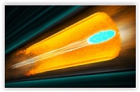
A team led by scientists from the University of California, Los Angeles and the Department of Energy’s SLAC National Accelerator Laboratory has reached another milestone in developing a promising technology for accelerating particles to high energies in short distances: They created a tiny tube of hot, ionized gas, or plasma, in which the particles remain tightly focused as they fly through it.
The technique is especially important for positrons, the antimatter siblings of electrons, which tend to lose focus as they travel through plasma during a process known as plasma wakefield acceleration. In tests at SLAC’s Facility for Advanced Accelerator Experimental Tests (FACET), a DOE Office of Science User Facility, beams of positrons stayed tightly bundled as they traveled through the plasma tube.
“Being able to efficiently create particle beams that are both highly energetic and focused is a prerequisite for many state-of-the-art accelerator applications,” says SLAC’s Marc Hogan, co-principal investigator of a study published today in Nature Communications. “Our results bring us a step closer to making plasma-driven particle accelerators a reality.”
Such devices could potentially power future particle colliders that reveal nature’s fundamental components, as well as bright X-ray light sources that take ultrafast snapshots of materials with atomic resolution.
A Plasma Tube to Keep Speedy Particles on Track
In plasma wakefield acceleration, energetic bundles of electrons or positrons traverse a plasma and generate plasma “wakes” for trailing bunches of particles to ride. Since the method can boost the energy of the surfing particles up to 1,000 times more over a given distance than conventional technology, it could pave the way for next-generation accelerators that are more powerful, smaller and less expensive.
However, the technique has yet to overcome a major challenge: Strong forces pointing toward the center of the plasma can degrade the quality of the particle beam, which consists of bunches of electrons or positrons. In the positron case, the particles are defocused and lost in the plasma.
Now, says SLAC’s Spencer Gessner, the lead author of the new study, “We’ve engineered a hollow plasma channel – a tube of plasma with neutral gas on the inside. Due to the particular geometry of the plasma, particles flying through the channel don’t experience any of the unwanted forces.”
Proof-of-Principle Experiment at FACET
The idea of creating plasma tubes has been around for about 20 years, but Gessner and his fellow researchers are the first to demonstrate that they can actually make these channels large enough for particle acceleration experiments.
To create plasma for their experiments, the researchers send a high-power laser through a hot gas of the chemical element lithium. Normally, the laser beam’s intensity is rather uniform and therefore generates a uniform plasma.
But in this case, they first sent the beam through a special spiral-shaped grating, which shaped the laser beam in such a way that if you looked at it in cross-section, it would consist of concentric rings. The innermost ring was the only one intense enough to create plasma, and as the laser beam traveled through a cloud of lithium gas, this ring formed a plasma tube about 3 inches long and two-hundredths of an inch wide. The tube persisted for just a few trillionths of a second – long enough for the scientists to send one of FACET’s powerful positron beams through it.
“Our results indeed show that the positron bunch doesn’t get defocused as it travels through the tube,” Gessner says. “But we found even more: The plasma responds by producing a wake that takes a lot of energy out of the bunch. This energy could be used to accelerate a trailing bunch of positrons.”
Next Steps Toward Future Applications
The team will soon follow up with experiments aimed at demonstrating that the technique can in fact boost the energy of positrons that surf the plasma wave inside the hollow channel. The researchers also intend to improve the method’s efficiency by increasing the amount of energy stored in the wake, which already corresponds to 10 times the acceleration power of conventional radiofrequency acceleration technology.
“With its unique combination of powerful positron beams and high-power lasers, FACET is the only place in the world where we can do this type of research,” Hogan says. “We’re looking forward to further exploring this exciting approach to plasma wakefield acceleration.”
In addition to UCLA and SLAC, the following institutions contributed to this work: University of Oslo, Norway; University of Paris-Saclay, France; and Tsinghua University, China. The project received funding from the DOE, the Research Council of Norway, the National Science Foundation, the European Research Council and the National Basic Research Program of China.
Share on:


Testimonial
"In a year when every marketing dollar mattered, I chose to keep I-Connect007 in our 2025 plan. Their commitment to high-quality, insightful content aligns with Koh Young’s values and helps readers navigate a changing industry. "
Brent Fischthal - Koh YoungSuggested Items
Rules of Thumb: Design007 Magazine, November 2024
11/11/2024 | I-Connect007 Editorial TeamRules of thumb are everywhere, but there may be hundreds of rules of thumb for PCB design. They’re built on design formulas, fabricators’ limitations, and tribal knowledge. And unfortunately, some longtime rules of thumb should be avoided at all costs. How do we separate the wheat from the chaff, so to speak?
Connect the Dots: Best Practices for Prototyping
09/21/2023 | Matt Stevenson -- Column: Connect the DotsPCB prototyping is a critical juncture during an electronic device’s journey from concept to reality. Regardless of a project’s complexity, the process of transforming a design into a working board is often enlightening in terms of how a design can be improved before a PCB is ready for full production.
The Drive Toward UHDI and Substrates
09/20/2023 | I-Connect007 Editorial TeamPanasonic’s Darren Hitchcock spoke with the I-Connect007 Editorial Team on the complexities of moving toward ultra HDI manufacturing. As we learn in this conversation, the number of shifting constraints relative to traditional PCB fabrication is quite large and can sometimes conflict with each other.
Asia/Pacific AI Spending Surge to Reach a Projected $78 Billion by 2027
09/19/2023 | IDCAsia/Pacific spending on Artificial Intelligence (AI) ), including software, services, and hardware for AI-centric systems will grow to $78.4 billion in 2027, according to International Data Corporation's latest Worldwide Artificial Intelligence Spending Guide.
Intel to Sell Minority Stake in IMS Nanofabrication Business to TSMC
09/13/2023 | IntelIntel Corporation announced that it has agreed to sell an approximately 10% stake in the IMS Nanofabrication business to TSMC. TSMC’s investment values IMS at approximately $4.3 billion, consistent with the valuation of the recent stake sale to Bain Capital Special Situations.