


 SMT Perspectives & Prospects: Artificial Intelligence Part 6: Data Module 1
 Standard of Excellence: Overcoming Service Failures—The Art of the Apology
 Nolan’s Notes: Tariffs, Technologies, and Optimization


Saki Presents 3D AOI Side-Angle Optics and Lighting Technology at NEPCON Thailand
June 16, 2016 | Saki CorporationEstimated reading time: 1 minute
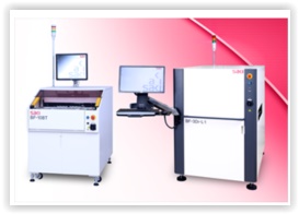
Saki Corporation, an innovator in the field of automated optical inspection equipment, will present its 3D automated optical inspection (AOI) equipment with innovative side-angle cameras and ring lighting technology at NEPCON Thailand 2016, held June 22-25, 2016, at BITEC in Bangkok, Thailand. Saki's 2D AOI system for simultaneous double-sided PCB inspection will also be on display.
Saki's BF-3Di-L1 3D AOI system has a new optical head, side-angle cameras, and 4-stage ring lighting for optimum illumination and better visual image capture and measurement of the printed circuit board assembly, for all PCB configurations. The circular lighting gives more consistent illumination throughout the field of view, with brightness controlled and shadows eliminated no matter the height or density of the components. Side cameras capture angles to show side views that previously weren't visible. The result is improved accuracy and reliability. This system inspects heights up to 20mm and parts as small as 01005s, capturing reversed or inclined components with an escape of less than 1 ppm. It can be used for simple set-ups, like golden board comparisons, or with its full algorithm-based capabilities for full measurement and inspection.
The BF-10BT 2D offline AOI system simultaneously inspects both sides of the circuit board with user-selectable 10μm and 20μm dual-resolution, for the ultimate in double-sided PCB inspection. Its robust and highly repeatable hardware is built for 24/7 continuous operation. It inspects 01005 (0402) components and detects solder balls down to 150 microns with high speed and superior data handling. It can be used for final inspection, through-hole inspection after wave or selective soldering, or manual inspection.
"Exhibiting at NEPCON Thailand is a great way for us to show our new AOI systems to a larger number of people in Thailand and the Asia Pacific region," said Francis Wong, managing director of Saki Asia Pacific, Thailand. "Thailand has long been an important market for Saki. We have both an office and sales rep here."
For more information contact Saki Asia Pacific, Thailand at all.th@sakicorp.com.
About Saki Corporation
Since its inception in 1994, Saki has led the way in the development of automatic recognition through robotic vision technology, applying ground-breaking image processing tools to solve inspection problems associated with printed circuit board assembly. Saki Corporation has headquarters in Tokyo, Japan with offices and sales and support centers around the world. Saki has Quality Management System JIS Q 9001:2008 and ISO 9001:2008 certifications.
Share on:


Testimonial
"We’re proud to call I-Connect007 a trusted partner. Their innovative approach and industry insight made our podcast collaboration a success by connecting us with the right audience and delivering real results."
Julia McCaffrey - NCAB GroupSuggested Items
Indium to Showcase High-Reliability Solder and Flux-Cored Wire Solutions at SMTA International
10/09/2025 | Indium CorporationAs one of the leading materials providers in the electronics industry, Indium Corporation® will feature its innovative, high-reliability solder and flux-cored wire products at SMTA International (SMTAI), to be held October 19-23 in Rosemont, Illinois.
‘Create your Connections’ – Rehm at productronica 2025 in Munich
10/08/2025 | Rehm Thermal SystemsThe electronics industry is undergoing dynamic transformation: smart production lines, sustainability, artificial intelligence, and sensor technologies dominate current discussions.
Amplifying Innovation: New Podcast Series Spotlights Electronics Industry Leaders
10/08/2025 | I-Connect007In the debut episode, “Building Reliability: KOKI’s Approach to Solder Joint Challenges,” host Marcy LaRont speaks with Shantanu Joshi, Head of Customer Solutions and Operational Excellence at KOKI Solder America. They explore how advanced materials, such as crack-free fluxes and zero-flux-residue solder pastes, are addressing issues like voiding, heat dissipation, and solder joint reliability in demanding applications, where failure can result in costly repairs or even catastrophic loss.
SASinno Americas Introduces the Ultra Series
10/07/2025 | SASinno AmericasSASinno Americas has introduced the new Ultra Series, the latest generation of offline selective soldering systems. Available in two models—the Ultra-i1 and Ultra-i2—the new series is designed to meet the needs of manufacturers running small to medium batch sizes, multiple product types, and frequent line changes, while maintaining exceptional precision and process control.
Elmotec by E-Tronix to Showcase SolderSmart® TOP Robotic Soldering at The Assembly Show 2025
10/06/2025 | ELMOTECE-tronix, a Stromberg Company, is pleased to announce its participation at The Assembly Show 2025 in Rosemont, IL, October 21st through 23rd. Exhibiting under Elmotec by E-Tronix, Booth #448, the team will highlight the SolderSmart® TOP robotic soldering system, featuring live demonstrations throughout the show.