


 Dan’s Biz Bookshelf: Four Important Books You Need to Read (Not Just Say You Have)
 The Marketing Minute: Cracking the Code of Technical Marketing


New Generation of High-efficiency Solar Thermal Absorbers Developed
June 16, 2016 | University of BristolEstimated reading time: 1 minute
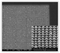
Researchers from the Universities of Bristol and Exeter are one step closer to developing a new generation of low-cost, high-efficiency solar cells. The structure is one of the world's first examples of a tri-layer metasurface absorber using a carbon interlayer.
The system, developed by Chenglong Wang a PhD student in Professor Martin Cryan's research group, uses amorphous carbon as an inter-layer between thin gold films with the upper film patterned with a 2D periodic array using focused ion beam etching.
The trilayer gold-carbon-gold metasurface strongly absorbs light across the solar spectrum but minimises emission of thermal radiation from the structure. The use of gold in the research is a first step towards a high temperature metasurface where gold can be replaced by other refractory metals such as tungsten or chrome.
The cell will be used for solar thermal energy applications and has the potential to reach much higher temperatures than simple black surfaces because it can minimise the emission of thermal radiation.
The metasurface has been developed as part of a joint project, led by Dr Neil Fox, between Bristol's Department of Electrical and Electronic Engineering and Schools of Physics and Chemistry. The aim of this project is to develop diamond-based solar thermionic devices, which use sunlight to get surfaces sufficiently hot that they emit electrons directly into a vacuum. If these electrons are collected at a cooled anode, electrical energy can be produced with maximum efficiencies predicted to be much higher than is achievable using conventional silicon solar cells.
Martin Cryan, Professor of Applied Electromagnetics and Photonics in the Department of Electrical and Electronic Engineering, said: "Integrating diamond within metasurfaces is very challenging, and this paper is a first step in that direction using amorphous carbon. The next stage is to carry out high temperature testing on the structures and to attempt to reach the ~700 degrees celsius required to obtain efficient thermionic emission."
The Bristol team have been working with Professor Tapas Mallick from the University of Exeter to develop the low-cost solar concentrator systems.
Share on:


Testimonial
"We’re proud to call I-Connect007 a trusted partner. Their innovative approach and industry insight made our podcast collaboration a success by connecting us with the right audience and delivering real results."
Julia McCaffrey - NCAB GroupSuggested Items
Closing the Loop on PCB Etching Waste
09/09/2025 | Shawn Stone, IECAs the PCB industry continues its push toward greener, more cost-efficient operations, Sigma Engineering’s Mecer System offers a comprehensive solution to two of the industry’s most persistent pain points: etchant consumption and rinse water waste. Designed as a modular, fully automated platform, the Mecer System regenerates spent copper etchants—both alkaline and acidic—and simultaneously recycles rinse water, transforming a traditionally linear chemical process into a closed-loop system.
The Chemical Connection: Through-glass Vias in Glass Substrates
06/24/2025 | Don Ball -- Column: The Chemical ConnectionThis month’s theme is vias and how best to ensure via quality and reliability. I don’t have much expertise in this process area or much to contribute that most of you don’t already know. However, I’ve recently become peripherally involved in a via technology that may be of more than academic interest to some of us. It entails putting vias in a material not usually associated with PCB manufacturing: through-glass vias (TGVs) in glass substrates.
In Pursuit of Perfection: Defect Reduction—May 2025 PCB007 Magazine Now Available
05/15/2025 | I-Connect007 Editorial TeamFor bare PCB board fabrication, defect reduction is a critical aspect of a company's bottom line profitability. In the May 2025 issue of PCB007 Magazine, we examine the imaging, etching, and plating processes, as well as product traceability on the shop floor, providing information and insight into how you can reduce your defects and increase yields.
DuPont to Showcase Advanced Semiconductor Wet Etching Innovations at the Surface Preparation and Cleaning Conference
05/13/2025 | DuPontDuPont announced that it will present its latest developments in semiconductor wet etching technologies at the upcoming Surface Preparation and Cleaning Conference (SPCC) in Chandler, Arizona, beginning May 20.
The Chemical Connection: Common Misconceptions in Wet Processing
04/28/2025 | Don Ball -- Column: The Chemical ConnectionInitially, I thought an April Fool’s column would be fun this month. I could highlight some of the crazier ideas and misconceptions I’ve witnessed over the years from potential customers and we could all have a good laugh. For example, there was a first-time buyer of a ferric chloride etcher (with no regeneration system) who was astonished to learn that he had to put fresh etchant in the system occasionally to maintain production.