


 Dan’s Biz Bookshelf: Four Important Books You Need to Read (Not Just Say You Have)
 The Marketing Minute: Cracking the Code of Technical Marketing


Terahertz Radiation: A Useful Source for Food Safety
June 20, 2016 | MAX-PLANCK-GESELLSCHAFTEstimated reading time: 3 minutes
An effective and less expensive tool for the inspection of food and drugs could soon be a reality. Scientists from the Fritz Haber Institute of the Max Planck Society in Berlin have been working with national and international partners to develop a conceptually new source of terahertz radiation. The innovation makes it much easier to generate this radiation, which is well suited to the analysis of soft materials and could therefore be more widely used in the food and pharmaceutical industry in future.
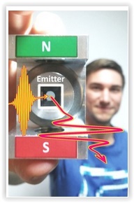
Compact and low cost: Max Planck researchers have developed a new source of radiation across the entire terahertz spectrum that is expected to enable new applications for this radiation.
Terahertz waves lie in the frequency range between from about 0.3 to 30 terahertz in the electromagnetic spectrum – between microwaves and infrared light. They are useful for analyzing organic materials, as they can penetrate things like textiles and plastics while also being characteristically absorbed by many pharmaceuticals. Unlike X-rays or other sources of radiation, terahertz radiation is also completely harmless for the body.
A large bandwidth for the food and pharmaceutical industry
“Our method of generating terahertz radiation makes applications possible that were previously too costly for such sources,” says Tobias Kampfrath, leader of the Terahertz Physics Research Group at the Fritz Haber Institute, which spearheaded the development process. The terahertz source which Kampfrath’s team and their partners in Mainz, Greifswald and Jülich, as well as in the US, Sweden and France, have now presented is the first to generate the entire bandwidth of terahertz radiation at relatively low cost. This could be extremely useful for the inspection of food and drugs, as analyses with broadband terahertz radiation target numerous substances and thus deliver more meaningful results. Currently, equipment which can generate the entire spectrum of terahertz radiation is still big and expensive, as it relies on very powerful lasers.
“Our emitter generates the entire spectrum from 1 to 30 terahertz and is therefore also suitable for use as a table-top emitter. Not only that; it is more energy efficient, easier to operate and cheaper to manufacture than former sources,” according to Tom Seifert, doctoral student at the Fritz Haber Institute. “We anticipate that it will quickly find use on a broad basis.”
A short pulse of current turns a metallic bilayer into an antenna
The source is powered by a compact femtosecond laser, which generates 80 million ultrashort flashes of light per second. It excites the actual emitter, which resembles a solar cell. However, it consists of two metal layers, one magnetic and one non-magnetic, each just three nanometers thick, which are grown on a glass substrate. When an ultrashort laser pulse hits the material, it generates a current burst, turning the metallic bilayer into a type of antenna emitting electromagnetic waves with terahertz frequencies.
“The emitter works so well because, in addition to the charge of the flowing electrons, we also use their spin,” explains Tom Seifert. The spin of an electron is a magnetic property which can have two distinct values. It causes the current to behave differently in magnetic than in non-magnetic metals. First, the laser light excites different numbers of electrons with the two possible spin directions in the magnetic layer. Then, the current flows into the non-magnetic layer, where the electrons are deflected into opposite directions depending on their spin. This produces a current perpendicular to the electrons’ original direction of movement. It is precisely this current burst that then generates the terahertz pulse. Eventually, because the metallic bilayer is extremely thin, the electromagnetic radiation is barely weakened at all on its way out of the metal, as would be the case in a thicker layer
Share on:


Testimonial
"We’re proud to call I-Connect007 a trusted partner. Their innovative approach and industry insight made our podcast collaboration a success by connecting us with the right audience and delivering real results."
Julia McCaffrey - NCAB GroupSuggested Items
Rules of Thumb: Design007 Magazine, November 2024
11/11/2024 | I-Connect007 Editorial TeamRules of thumb are everywhere, but there may be hundreds of rules of thumb for PCB design. They’re built on design formulas, fabricators’ limitations, and tribal knowledge. And unfortunately, some longtime rules of thumb should be avoided at all costs. How do we separate the wheat from the chaff, so to speak?
Connect the Dots: Best Practices for Prototyping
09/21/2023 | Matt Stevenson -- Column: Connect the DotsPCB prototyping is a critical juncture during an electronic device’s journey from concept to reality. Regardless of a project’s complexity, the process of transforming a design into a working board is often enlightening in terms of how a design can be improved before a PCB is ready for full production.
The Drive Toward UHDI and Substrates
09/20/2023 | I-Connect007 Editorial TeamPanasonic’s Darren Hitchcock spoke with the I-Connect007 Editorial Team on the complexities of moving toward ultra HDI manufacturing. As we learn in this conversation, the number of shifting constraints relative to traditional PCB fabrication is quite large and can sometimes conflict with each other.
Asia/Pacific AI Spending Surge to Reach a Projected $78 Billion by 2027
09/19/2023 | IDCAsia/Pacific spending on Artificial Intelligence (AI) ), including software, services, and hardware for AI-centric systems will grow to $78.4 billion in 2027, according to International Data Corporation's latest Worldwide Artificial Intelligence Spending Guide.
Intel to Sell Minority Stake in IMS Nanofabrication Business to TSMC
09/13/2023 | IntelIntel Corporation announced that it has agreed to sell an approximately 10% stake in the IMS Nanofabrication business to TSMC. TSMC’s investment values IMS at approximately $4.3 billion, consistent with the valuation of the recent stake sale to Bain Capital Special Situations.