


 Dan’s Biz Bookshelf: Four Important Books You Need to Read (Not Just Say You Have)
 The Marketing Minute: Cracking the Code of Technical Marketing


Proper Breeding Ground for Germanene
June 27, 2016 | University of TwenteEstimated reading time: 2 minutes
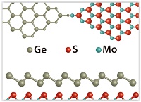
Graphene may currently be the best known ‘two dimensional’ material, its new cousin germanene seems to have properties that are even more attractive for application in electronics. For this, germanene has to grow in a one atom layer on top of a proper carrier - substrate. Scientists of the MESA+ Institute for Nanotechnology of the University of Twente managed to grow germanene on a semiconductor material, preserving the unique properties.
Germanene is a one atom thick sheet of germanium, in a honeycomb structure. It has clear similarities with graphene, the material that induced massive research activity worldwide, especially after 2010’s Nobel Prize. A major difference between graphene and germanene is the ‘band gap’, a property well-known in semiconductor electronics: thanks to this ‘jump’ of energy levels that electrons are allowed to have, it is possible to control, switch and amplify currents. Graphene had a very small band gap that can only be measured at very low temperatures, germanene shows a band gap that is significantly larger. Previous attempts to grow germanene, however, show that these attractive properties seem to vanish when it is grown on a metal surface: a good conductor of current. To prevent this, the UT scientists chose the semiconductor MoS2 as the substrate material.
Islands
Under ultra-high vacuum conditions, germanene indeed grows on the semiconductor. At first, the scientists observed islands at the locations where MoS2 had crystal defects, after that the germanene is spreading out covering a larger surface. An exciting question is, if the desired properties remain intact. First measurements show that the typical 2D properties and band gap are present, further low temperature measurements are needed to confirm that germanene operates in the desired way: the inner part would work as an insulator, while conducting channels are formed at the edges.
Sandwich
The other UT scientists did quantum mechanical calculations on the molybdenum-disulfide combination. They, for example, looked at the direction of growth, to be able to optimize the process. The theoretical group went one step further, by not only investigating the bilayer of molybdenum-disulfide, but als covering the germane with molybdeendisulfide. This prevents germanene from rapid oxidation. Calculations show that the sandwich construction has even better performance when it comes to the band gap.
Both publications show dat germanene, grown on molybdenum-disulfide is an important first step towards new electronic devices or unsuspected combinations with conventional devices. ‘Spintronics’, based on the spin movement of electrons, seems to be an attractive application area for germanene. Electrons with spin up and electrons with spin down have separate conducting channels on the edges of germanene. Harold Zandvliet recently received a grant for further research on this promising effect.
Share on:


Testimonial
"Advertising in PCB007 Magazine has been a great way to showcase our bare board testers to the right audience. The I-Connect007 team makes the process smooth and professional. We’re proud to be featured in such a trusted publication."
Klaus Koziol - atgSuggested Items
iDEAL Semiconductor Announces Polar Semiconductor as Manufacturing Partner for SuperQ™ Power Devices
09/18/2025 | PRNewswireiDEAL Semiconductor confirms that its ultra-efficient SuperQ™ silicon power devices are now in production at Polar Semiconductor, a leading foundry specializing in high-voltage, power, and sensor technologies.
Global Interposer Market to Surge Nearly Fivefold by 2034
09/15/2025 | I-Connect007 Editorial TeamRevenue for the global interposer market is projected to climb from $471 million in 2025 to more than $2.3 billion by 2034, according to a new report from Business Research Insights. The growth represents a CAGR of nearly 20 percent over the forecast period.
Zhen Ding Drives AI-Powered Digital Transformation
09/12/2025 | Zhen DingDriven by the surging demand for computing power fueled by AI, the semiconductor and PCB industries are forging closer integration, expanding their ecosystems, and pursuing shared growth. PCB has already become another NT$ trillion-dollar industry in Taiwan, growing in tandem with the semiconductor sector.
Zhen Ding Expands PCB into Semiconductors at SEMICON Taiwan 2025; Advantech Drives AI Smart Parks
09/12/2025 | Zhen DingZhen Ding Technology Holding Co., Ltd., a global leader in the PCB industry, returned to exhibit at SEMICON Taiwan 2025. Positioning itself as an industry pioneer in "PCB expanding into semiconductors," the company showcased its latest strategic layout
SkyWater Completes Acquisition of Fab 25, Expanding U.S. Pure-Play Foundry Capacity for Critical Semiconductor Technologies
09/12/2025 | SkyWaterSkyWater Technology, the trusted technology realization partner, announced that it has completed its acquisition of Infineon Technologies AG’s 200 mm semiconductor fab in Austin, Texas (“Fab 25”)