


 Dan’s Biz Bookshelf: Four Important Books You Need to Read (Not Just Say You Have)
 The Marketing Minute: Cracking the Code of Technical Marketing


Graphene Could Revolutionize the Internet of Things
July 8, 2016 | EPFLEstimated reading time: 3 minutes
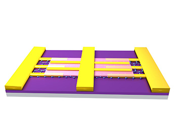
EPFL researchers have produced a tunable, graphene-based device that could significantly increase the speed and efficiency of wireless communication systems. Their system works at very high frequencies, delivering unprecedented results.
Wireless communications come in many forms - such as mobile phones using 4G or 5G connectivity, GPS devices, and computers connected via Bluetooth to portable sensors - and operate in different frequency bands. To work across multiple platforms, connected objects have to be compatible with a whole range of frequencies without being weighed down by excessive hardware.
Most portable, wireless systems currently come equipped with reconfigurable circuits that can adjust the antenna to transmit and receive data in the various frequency bands. The only problem is that the technologies currently available like MEMS and MOS, using silicon or metal, do not work well at high frequencies. And that's where data can travel much faster.
The new graphene-based solution, which was developed in the Nanoelectronic Devices Laboratory, is designed to replace tunable capacitors, which can be found in all wireless devices. The new device "tunes" the circuits to different frequencies so that they can operate across a wide range of frequency bands. It also meets other needs that neither MEMS nor MOS capacitors can: good performance at high frequency, miniaturization and the ability to be tuned using low energy.
The EPFL researchers overcame these obstacles with a graphene-based capacitor that is compatible with traditional circuits. The device consumes very little energy and, above 2.1 GHz, easily outperforms its competitors and has a miniaturized design. "The surface area of a conventional MEMS system would have to be a thousand times greater to get the capacitance value," said Clara Moldovan.
How does it work?
The researchers' breakthrough is based on a clever sandwich structure that takes graphene's unique characteristics into account. "When graphene was discovered more than 10 years ago, it caused a real stir," said Moldovan. "It was considered a miracle material: it is a very good electrical and thermal conductor and it is flexible, lightweight, transparent and sturdy. But researchers discovered that it was difficult to integrate into electronic systems because its atomic thickness gives it high effective resistance."
The sandwich-shaped structure takes advantage of the fact that a two-dimensional gas of electrons in a quantum well can behave like a quantum capacitance. This is because it follows the Pauli Exclusion Principle, according to which a certain amount of energy is needed to fill a quantum well with electrons. Quantum capacitance can be easily measured in a single-atom layer of graphene, and the key advantage is that it is tunable by varying the charge density in graphene with a very low voltage.
"It's by applying voltage that we can ‘tune' our capacitors to a given frequency, just like tuning a radio to get different stations," said Moldovan, the lead author of the article.
Many advantages
The EPFL researchers' device, which is only several hundred micrometers (around 0.05 cm) long and wide, can be stiff or flexible, is easily miniaturized, and uses very little energy. Potential applications are numerous. In addition to improving the flow of data between connected devices, it could extend battery life and lead to ever more compact devices. In its flexible state, it could be easily used in sensors placed in clothes or directly on the human body. "Our results confirm that graphene could truly revolutionize the future of wireless communications," said Moldovan.
The end technology will be a hybrid in which graphene will be paired with advanced silicon technologies. "Some have claimed that graphene will one day replace silicon technology," said Adrian Ionescu, the head of the Nanolab. "But in reality, graphene is most effective in the realm of electronics when it is combined with functional silicon blocks."
Share on:


Testimonial
"We’re proud to call I-Connect007 a trusted partner. Their innovative approach and industry insight made our podcast collaboration a success by connecting us with the right audience and delivering real results."
Julia McCaffrey - NCAB GroupSuggested Items
Rules of Thumb: Design007 Magazine, November 2024
11/11/2024 | I-Connect007 Editorial TeamRules of thumb are everywhere, but there may be hundreds of rules of thumb for PCB design. They’re built on design formulas, fabricators’ limitations, and tribal knowledge. And unfortunately, some longtime rules of thumb should be avoided at all costs. How do we separate the wheat from the chaff, so to speak?
Connect the Dots: Best Practices for Prototyping
09/21/2023 | Matt Stevenson -- Column: Connect the DotsPCB prototyping is a critical juncture during an electronic device’s journey from concept to reality. Regardless of a project’s complexity, the process of transforming a design into a working board is often enlightening in terms of how a design can be improved before a PCB is ready for full production.
The Drive Toward UHDI and Substrates
09/20/2023 | I-Connect007 Editorial TeamPanasonic’s Darren Hitchcock spoke with the I-Connect007 Editorial Team on the complexities of moving toward ultra HDI manufacturing. As we learn in this conversation, the number of shifting constraints relative to traditional PCB fabrication is quite large and can sometimes conflict with each other.
Asia/Pacific AI Spending Surge to Reach a Projected $78 Billion by 2027
09/19/2023 | IDCAsia/Pacific spending on Artificial Intelligence (AI) ), including software, services, and hardware for AI-centric systems will grow to $78.4 billion in 2027, according to International Data Corporation's latest Worldwide Artificial Intelligence Spending Guide.
Intel to Sell Minority Stake in IMS Nanofabrication Business to TSMC
09/13/2023 | IntelIntel Corporation announced that it has agreed to sell an approximately 10% stake in the IMS Nanofabrication business to TSMC. TSMC’s investment values IMS at approximately $4.3 billion, consistent with the valuation of the recent stake sale to Bain Capital Special Situations.