


 Dan’s Biz Bookshelf: Four Important Books You Need to Read (Not Just Say You Have)
 The Marketing Minute: Cracking the Code of Technical Marketing


Watch Out, Silicon Chips. Molecular Electronics Are Coming
July 12, 2016 | ATSEstimated reading time: 3 minutes
Technion researchers have developed a method for growing carbon nanotubes that could lead to the day when molecular electronics replace the ubiquitous silicon chip as the building block of electronics.
Carbon nanotubes (CNTs) have long fascinated scientists because of their unprecedented electrical, optical, thermal and mechanical properties, and chemical sensitivity. But significant challenges remain before CNTs can be implemented on a wide scale, including the need to produce them in specific locations on a smooth substrate, in conditions that will lead to the formation of a circuit around them.
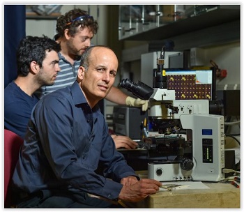
Led by Prof. Yuval Yaish of the Viterbi Faculty of Electrical Engineering and the Zisapel Nanoelectronics Center at the Technion, the researchers have developed a technology that addresses these challenges. Their breakthrough also makes it possible to study the dynamic properties of CNTs, including acceleration, resonance (vibration), and the transition from softness to hardness.
The method could serve as an applicable platform for the integration of nano-electronics with silicon technologies, and possibly even the replacement of these technologies in molecular electronics.
“The CNT is an amazing and very strong building block with remarkable electrical, mechanical and optical properties,” said Prof. Yaish. “Some are conductors, and some are semiconductors, which is why they are considered a future replacement for silicon. But current methods for the production of CNTs are slow, costly, and imprecise. As such, they generally cannot be implemented in industry.”
Preferential adsorption of p-nitrobenzoic acid on carbon nanotubes. (a) Top: Chemical structure of p-nitrobenzoic acid (pNBA). Bottom: Schematic illustration of the monoclinic unit cell of pNBA powder as extracted from X-ray diffraction analysis. (b,c) Dark field optical microscopy images of pNBA nanocrystals adsorbed along CVD grown carbon nanotubes (CNTs). Scale bar, 50 and 20 µm, respectively. (d) Amplitude image of AFM of a single CNT with a few pNBA nanocrystals along. Scale bar, 1 µm. Inset: height cross sections along the marked lines of the main figure. (e) Dark field optical microscopy image of pNBA nanocrystals after intensive deposition. Note the black voids along the CNT. Scale bar, 20 µm. (f) Dark field optical microscopy image of pNBA nanocrystals adsorb onto commercial dispersed CNTs. Scale bar, 20 µm.
Due to the nanometer size of the CNTs (100,000 times smaller in diameter than the thickness of a human hair) it is extremely difficult to find or locate them at specific locations. Prof. Yaish, and graduate students Gilad Zeevi and Michael Shlafman, developed a simple, rapid, non-invasive and scalable technique that enables optical imaging of CNTs. Instead of depending upon the CNT chemical properties to bind marker molecules, the researchers relied on the fact that the CNT is both a chemical and physical defect on the otherwise flat and uniform surface. It can serve as a seed for the nucleation and growth of small, but optically visible nanocrystals, which can be seen and studied using a conventional optical microscope (CNTs, because of their small size, are too small to be seen in this way). Since the CNT surface is not used to bind the molecules, they can be removed completely after imaging, leaving the surface intact, and preserving the CNT’s electrical and mechanical properties.
“Our approach is the opposite of the norm,” he continued. “We grow the CNTs directly, and with the aid of the organic crystals that coat them, we can see them under a microscope very quickly. Then image identification software finds and produces the device (transistor). This is the strategy. The goal is to integrate CNTs in an integrated circuit of miniaturized electronic components (mainly transistors) on a single chip (VLSI). These could one day serve as a replacement for silicon electronics.”
Prof. Yaish also noted that the ability to demonstrate this principle and create world-class devices was made possible by the unique infrastructures available at the Technion clean room facilities in the Wolfson Microelectronics Center, headed by Prof. Nir Tessler.
Share on:


Testimonial
"Our marketing partnership with I-Connect007 is already delivering. Just a day after our press release went live, we received a direct inquiry about our updated products!"
Rachael Temple - AlltematedSuggested Items
MEMS & Imaging Sensors Summit to Spotlight Sensing Revolution for Europe’s Leadership
09/11/2025 | SEMIIndustry experts will gather November 19-20 at the SEMI MEMS & Imaging Sensors Summit 2025 to explore the latest breakthroughs in AI-driven MEMS and imaging optimization, AR/VR technologies, and advanced sensor solutions for critical defence applications.
Direct Imaging System Market Size to Hit $4.30B by 2032, Driven by Increasing Demand for High-Precision PCB Manufacturing
09/11/2025 | Globe NewswireAccording to the SNS Insider, “The Direct Imaging System Market size was valued at $2.21 Billion in 2024 and is projected to reach $4.30 Billion by 2032, growing at a CAGR of 8.68% during 2025-2032.”
I-Connect007’s Editor’s Choice: Five Must-Reads for the Week
07/04/2025 | Marcy LaRont, I-Connect007For our industry, we have seen several bullish market announcements over the past few weeks, including one this week by IDC on the massive growth in the global server market. We’re also closely watching global trade and nearshoring. One good example of successful nearshoring is Rehm Thermal Systems, which celebrates its 10th anniversary in Mexico and the official opening of its new building in Guadalajara.
Driving Innovation: Direct Imaging vs. Conventional Exposure
07/01/2025 | Simon Khesin -- Column: Driving InnovationMy first camera used Kodak film. I even experimented with developing photos in the bathroom, though I usually dropped the film off at a Kodak center and received the prints two weeks later, only to discover that some images were out of focus or poorly framed. Today, every smartphone contains a high-quality camera capable of producing stunning images instantly.
United Electronics Corporation Advances Manufacturing Capabilities with Schmoll MDI-ST Imaging Equipment
06/24/2025 | United Electronics CorporationUnited Electronics Corporation has successfully installed the advanced Schmoll MDI-ST (XL) imaging equipment at their advanced printed circuit board facility. This significant technology investment represents a continued commitment to delivering superior products and maintaining their position as an industry leader in precision PCB manufacturing.