


 Dan’s Biz Bookshelf: Four Important Books You Need to Read (Not Just Say You Have)
 The Marketing Minute: Cracking the Code of Technical Marketing


Engineers Integrate Nano-scale Sensors, Electronics and Microfluidics into Threads
July 22, 2016 | Tufts UniversityEstimated reading time: 3 minutes
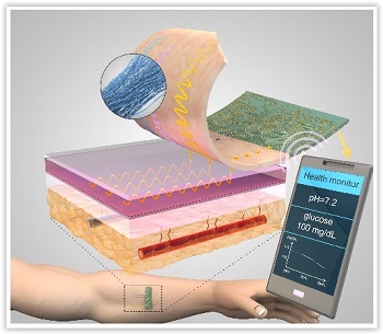
For the first time, researchers led by Tufts University engineers have integrated nano-scale sensors, electronics and microfluidics into threads – ranging from simple cotton to sophisticated synthetics – that can be sutured through multiple layers of tissue to gather diagnostic data wirelessly in real time, according to a paper published online July 18 in Microsystems & Nanoengineering. The research suggests that the thread-based diagnostic platform could be an effective substrate for a new generation of implantable diagnostic devices and smart wearable systems.
The researchers used a variety of conductive threads that were dipped in physical and chemical sensing compounds and connected to wireless electronic circuitry to create a flexible platform that they sutured into tissue in rats as well as in vitro. The threads collected data on tissue health (e.g. pressure, stress, strain and temperature), pH and glucose levels that can be used to determine such things as how a wound is healing, whether infection is emerging, or whether the body’s chemistry is out of balance. The results were transmitted wirelessly to a cell phone and computer.
The three-dimensional platform is able to conform to complex structures such as organs, wounds or orthopedic implants.
While more study is needed in a number of areas, including investigation of long-term biocompatibility, researchers said initial results raise the possibility of optimizing patient-specific treatments.
“The ability to suture a thread-based diagnostic device intimately in a tissue or organ environment in three dimensions adds a unique feature that is not available with other flexible diagnostic platforms,” said Sameer Sonkusale, Ph.D., corresponding author on the paper and director of the interdisciplinary Nano Lab in the Department of Electrical and Computer Engineering at Tufts School of Engineering. “We think thread-based devices could potentially be used as smart sutures for surgical implants, smart bandages to monitor wound healing, or integrated with textile or fabric as personalized health monitors and point-of-care diagnostics.”
Until now, the structure of substrates for implantable devices has essentially been two-dimensional, limiting their usefulness to flat tissue such as skin, according to the paper. Additionally, the materials in those substrates are expensive and require specialized processing.
“By contrast, thread is abundant, inexpensive, thin and flexible, and can be easily manipulated into complex shapes,” said Pooria Mostafalu, Ph.D., first author on the paper who was a doctoral student at Tufts when he worked on the project and is now a postdoctoral research fellow with the Harvard-MIT Division of Health Sciences and Technology, Brigham and Women’s Hospital, and the Wyss Institute for Biologically Inspired Engineering at Harvard University. “Additionally, analytes can be delivered directly to tissue by using thread’s natural wicking properties.”
Other authors on the paper were Kyle A. Alberti and Qiaobing Xu, both of the Tufts University Department of Biomedical Engineering; Mohsen Akbari and Ali Khademhosseini, both of Harvard Medical School’s Biomaterials Innovation Research Center, the Harvard-MIT Division of Health Science and Technology and Harvard University’s Wyss Institute for Biologically Inspired Engineering. Khademhosseini is also affiliated with King Abdulaziz University’s Department of Physics.
About Tufts University’s School of Engineering
Located on Tufts' Medford/Somerville campus, the School of Engineering offers a rigorous engineering education in a unique environment that blends the intellectual and technological resources of a world-class research university with the strengths of a top-ranked liberal arts college. Close partnerships with Tufts' excellent undergraduate, graduate and professional schools, coupled with a long tradition of collaboration, provide a strong platform for interdisciplinary education and scholarship. The School of Engineering’s mission is to educate engineers committed to the innovative and ethical application of science and technology in addressing the most pressing societal needs, to develop and nurture twenty-first century leadership qualities in its students, faculty, and alumni, and to create and disseminate transformational new knowledge and technologies that further the well-being and sustainability of society in such cross-cutting areas as human health, environmental sustainability, alternative energy, and the human-technology interface.
Share on:


Testimonial
"Advertising in PCB007 Magazine has been a great way to showcase our bare board testers to the right audience. The I-Connect007 team makes the process smooth and professional. We’re proud to be featured in such a trusted publication."
Klaus Koziol - atgSuggested Items
Blaize, Technology Control Company Partner to Power Saudi Arabia’s Next-Generation AI Innovation Infrastructure
09/17/2025 | BUSINESS WIREBlaize Holdings, Inc., a leader in programmable, energy-efficient edge AI computing, and Technology Control Company (TCC), a leading technology solutions provider in the Kingdom of Saudi Arabia (KSA), announced a strategic partnership to advance Saudi Arabia’s AI innovation infrastructure and accelerate its digital transformation goals.
BLT Joins Microchip Partner Program as Design Partner
09/17/2025 | BUSINESS WIREBLT, a U.S.-owned and operated engineering design services firm announced it has joined the Microchip Design Partner Program.
Curing and Verification in PCB Shadow Areas
09/17/2025 | Doug Katze, DymaxDesign engineers know a simple truth that often complicates electronics manufacturing: Light doesn’t go around corners. In densely populated PCBs, adhesives and coatings often fail to fully cure in shadowed regions created by tall ICs, connectors, relays, and tight housings.
On the Line With… Podcast: UHDI and RF Performance
09/17/2025 | I-Connect007I-Connect007 is excited to announce the release of a new episode in its latest On the Line with... podcast series, which shines a spotlight on one of the most important emerging innovations in electronics manufacturing: Ultra-High-Density Interconnect (UHDI).
Altair, Wichita State University’s NIAR Sign MoU to Accelerate Aerospace Innovation
09/16/2025 | AltairAltair, a global leader in computational intelligence, and Wichita State University’s (WSU) National Institute for Aviation Research (NIAR), one of the world’s leading aerospace research institutions, have signed a memorandum of understanding (MoU) to advance innovation across the aerospace and defense industries.