


 Dan’s Biz Bookshelf: Four Important Books You Need to Read (Not Just Say You Have)
 The Marketing Minute: Cracking the Code of Technical Marketing


New Nontoxic Process Promises Larger Ultrathin Sheets of 2D Nanomaterials
July 27, 2016 | ORNLEstimated reading time: 2 minutes
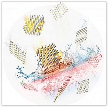
A team of scientists led by the Department of Energy’s Oak Ridge National Laboratory has developed a novel way to produce two-dimensional nanosheets by separating bulk materials with nontoxic liquid nitrogen. The environmentally friendly process generates a 20-fold increase in surface area per sheet, which could expand the nanomaterials’ commercial applications.
“It’s actually a very simple procedure,” said ORNL chemist Huiyuan Zhu, who co-authored a study published in Angewandte Chemie International Edition. “We heated commercially available boron nitride in a furnace to 800 degrees Celsius to expand the material’s 2D layers. Then, we immediately dipped the material into liquid nitrogen, which penetrates through the interlayers, gasifies into nitrogen, and exfoliates, or separates, the material into ultrathin layers.”
Nanosheets of boron nitride could be used in separation and catalysis, such as transforming carbon monoxide to carbon dioxide in gasoline-powered engines. They also may act as an absorbent to mop up hazardous waste. Zhu said the team’s controlled gas exfoliation process could be used to synthesize other 2D nanomaterials such as graphene, which has potential applications in semiconductors, photovoltaics, electrodes and water purification.
Because of the versatility and commercial potential of one-atom-thick 2D nanomaterials, scientists are seeking more efficient ways to produce larger sheets. Current exfoliation procedures use harsh chemicals that produce hazardous byproducts and reduce the amount of surface area per nanosheet, Zhu said.
“In this particular case, the surface area of the boron nitride nanosheets is 278 square meters per gram, and the commercially available boron nitride material has a surface area of only 10 square meters per gram,” Zhu said. “With 20 times more surface area, boron nitride can be used as a great support for catalysis.”
Further research is planned to expand the surface area of boron nitride nanosheets and also test their feasibility in cleaning up engine exhaust and improving the efficiency of hydrogen fuel cells.
Along with Zhu, several co-authors participated in the paper, “Controlled Gas Exfoliation of Boron Nitride into Few-Layered Nanosheets,” including ORNL’s Sheng Dai, Xiang Gao, Qian Li, Shannon M. Mahurin and Wenshuai Zhu; Yanhong Chao, Hongping Li and Huaming Li with Jiangsu University and Meijun Li from the University of Tennessee.
The study was supported by the DOE Office of Science. Additional funding was provided by the Liane Russell Distinguished Early Career Fellowship through the Laboratory Directed Research and Development program. Zhu joined ORNL in 2014 as one of the lab’s first Russell Fellows, and her primary area of research is on synthetic control of hybrid nanomaterials for catalytic applications.
Share on:


Testimonial
"The I-Connect007 team is outstanding—kind, responsive, and a true marketing partner. Their design team created fresh, eye-catching ads, and their editorial support polished our content to let our brand shine. Thank you all! "
Sweeney Ng - CEE PCBSuggested Items
Driving Innovation: Depth Routing Processes—Achieving Unparalleled Precision in Complex PCBs
09/08/2025 | Kurt Palmer -- Column: Driving InnovationIn PCB manufacturing, the demand for increasingly complex and miniaturized designs continually pushes the boundaries of traditional fabrication methods, including depth routing. Success in these applications demands not only on robust machinery but also sophisticated control functions. PCB manufacturers rely on advanced machine features and process methodologies to meet their precise depth routing goals. Here, I’ll explore some crucial functions that empower manufacturers to master complex depth routing challenges.
Polar Instruments Announces Additive Transmission Line Support for Si9000e
08/20/2025 | Polar InstrumentsTransmission lines embedded into the PCB surface are a feature of UHDI constructions. The 2025 fall release of Polar's Si9000e PCB impedance & insertion loss transmission line field solver incorporates eight new single ended, differential and coplanar transmission line structures.
Henniker Plasma Launches Stratus Turnkey Plasma Manufacturing Cell
08/13/2025 | Henniker PlasmaHenniker Plasma, a leading manufacturer of plasma treatment systems, proudly announces the launch of its Stratus Plasma Manufacturing Cell range — a fully integrated, turnkey solution that combines advanced atmospheric plasma surface treatment with robotic automation.
Trouble in Your Tank: Metallizing Flexible Circuit Materials—Mitigating Deposit Stress
08/04/2025 | Michael Carano -- Column: Trouble in Your TankMetallizing materials, such as polyimide used for flexible circuitry and high-reliability multilayer printed wiring boards, provide a significant challenge for process engineers. Conventional electroless copper systems often require pre-treatments with hazardous chemicals or have a small process window to achieve uniform coverage without blistering. It all boils down to enhancing the adhesion of the thin film of electroless copper to these smooth surfaces.
Designers Notebook: Basic PCB Planning Criteria—Establishing Design Constraints
07/22/2025 | Vern Solberg -- Column: Designer's NotebookPrinted circuit board development flows more smoothly when all critical issues are predefined and understood from the start. As a basic planning strategy, the designer must first consider the product performance criteria, then determine the specific industry standards or specifications that the product must meet. Planning also includes a review of all significant issues that may affect the product’s manufacture, performance, reliability, overall quality, and safety.