


 Dan’s Biz Bookshelf: Four Important Books You Need to Read (Not Just Say You Have)
 The Marketing Minute: Cracking the Code of Technical Marketing


Self-assembling Nano Inks Form Conductive and Transparent Grids During Imprint
July 28, 2016 | INMEstimated reading time: 1 minute
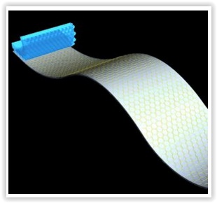
Transparent electronics devices are present in today’s thin film displays, solar cells, and touchscreens. The future will bring flexible versions of such devices. Their production requires printable materials that are transparent and remain highly conductive even when deformed. Researchers at INM – Leibniz Institute for New Materials have combined a new self-assembling nano ink with an imprint process to create flexible conductive grids with a resolution below one micrometer.
To print the grids, an ink of gold nanowires is applied to a substrate. A structured stamp is pressed on the substrate and forces the ink into a pattern. “The nanowires are extremely thin and flexible; they adapt to any pattern of the stamp. During drying, the individual wires self-assemble and form larger, percolating bundles that form the grid,” explains Tobias Kraus from INM. The stamp is removed and the grid is treated in a plasma. “This compresses the bundles into conductive wires and results in a transparent, conductive grid. Depending on the geometry of the stamp, this simple method can shape any nano or microgrid,” says Kraus, head of the program division Structure Formation.
The thickness of the grid can be controlled via the gold concentration. “Only very small quantities of gold are needed to produce a conductive grid, far less than when using inks with spherical gold particles,” says Kraus. This makes the advantages of gold accessible for flexible electronics.
“Our results show self-assembly and imprint can be combined to efficiently produce transparent, conductive materials. We will transfer this insight to other metals in further studies,” says Kraus.
INM conducts research and development to create new materials – for today, tomorrow and beyond. Chemists, physicists, biologists, materials scientists and engineers team up to focus on these essential questions: Which material properties are new, how can they be investigated and how can they be tailored for industrial applications in the future? Four research thrusts determine the current developments at INM: New materials for energy application, new concepts for medical surfaces, new surface materials for tribological systems and nano safety and nano bio. Research at INM is performed in three fields: Nanocomposite Technology, Interface Materials, and Bio Interfaces.
INM – Leibniz Institute for New Materials, situated in Saarbrücken, is an internationally leading centre for materials research. It is an institute of the Leibniz Association and has about 220 employees.
Share on:


Testimonial
"In a year when every marketing dollar mattered, I chose to keep I-Connect007 in our 2025 plan. Their commitment to high-quality, insightful content aligns with Koh Young’s values and helps readers navigate a changing industry. "
Brent Fischthal - Koh YoungSuggested Items
Curing and Verification in PCB Shadow Areas
09/17/2025 | Doug Katze, DymaxDesign engineers know a simple truth that often complicates electronics manufacturing: Light doesn’t go around corners. In densely populated PCBs, adhesives and coatings often fail to fully cure in shadowed regions created by tall ICs, connectors, relays, and tight housings.
Marcy’s Musings: Advancing the Advanced Materials Discussion
09/17/2025 | Marcy LaRont -- Column: Marcy's MusingsAs the industry’s most trusted global source of original content about the electronics supply chain, we continually ask you about your concerns, what you care about, and what you most want to learn about. Your responses are insightful and valuable. Thank you for caring enough to provide useful feedback and engage in dialogue.
September 2025 PCB007 Magazine: The Future of Advanced Materials
09/16/2025 | I-Connect007 Editorial TeamMoore’s Law is no more, and the advanced material solutions being developed to grapple with this reality are surprising, stunning, and perhaps a bit daunting. Buckle up for a dive into advanced materials and a glimpse into the next chapters of electronics manufacturing.
I-Connect007 Launches Advanced Electronics Packaging Digest
09/15/2025 | I-Connect007I-Connect007 is pleased to announce the launch of Advanced Electronics Packaging Digest (AEPD), a new monthly digital newsletter dedicated to one of the most critical and rapidly evolving areas of electronics manufacturing: advanced packaging at the interconnect level.
Panasonic Industry will Double the Production Capacity of MEGTRON Multi-layer Circuit Board Materials Over the Next Five Years
09/15/2025 | Panasonic Industry Co., Ltd.Panasonic Industry Co., Ltd., a Panasonic Group company, announced plans for a major expansion of its global production capacity for MEGTRON multi-layer circuit board materials today. The company plans to double its production over the next five years to meet growing demand in the AI server and ICT infrastructure markets.