


 Marcy’s Musing: From Pitch to PO—The Sales Stack
 It’s Only Common Sense: Knowing When to Walk Away
 Dan’s Biz Bookshelf: ‘Elevate: Push Beyond Your Limits'


Hybrid Solar Cells Have Applications in Flexible Electronics and Portable Devices
August 15, 2016 | KAUSTEstimated reading time: 2 minutes
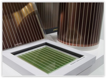
Understanding the impact of surface defects underpins the improved efficiency of hybrid organic/inorganic solar cells.
Hybrid solar cells utilize an interface comprising layers of organic and inorganic materials to convert sunlight into electricity. Zinc oxide (ZnO) is a popular choice for the inorganic material because it is cheap, non-toxic and readily available. However, the conversion efficiency of hybrid solar cells using ZnO/organic-donor bulk heterojunctions is currently very low—only 2 percent when ZnO is blended into an organic donor material. On the other hand, a decent 6.1 percent efficiency has been reached when ZnO is used as a layer sandwiched between an electrode and a layer of polymer or small-molecule acceptors.
Jean-Luc Bredas from the KAUST Solar & Photovoltaics Engineering Research Center and colleague Hong Li suspect that intrinsic defects in ZnO are a key factor in the poor performance1. By comparing the differences in electronic properties between various hybrid materials, they concluded that zinc vacancies reduce conversion efficiency by hindering the charge separation process at the interface between the organic and inorganic materials.
It is well known that ZnO adopts different roles in bulk heterojunctions depending on the type of organic material and architecture used. When blended with polymer or small-molecular donors such as sexithienyl, ZnO assumes the role of an electron acceptor: it takes up or "accepts" electrons and leaves positively charged holes behind in a sexithienyl layer.
When sandwiched between an electrode and a fullerene acceptor layer, ZnO helps transfer the electrons from the fullerene layer to the electrode. These processes enable the efficient conversion of sunlight into electricity.
The researchers used computer simulations to examine how zinc vacancies at the surface of zinc oxide impact these two processes. For the ZnO/sexithienyl bulk heterojunction, zinc vacancies at the ZnO surface can hinder local charge transfer at the ZnO/sexithienyl interface and can also prevent efficient charge separation due to strong Coulomb interactions. However, for the ZnO/fullerene interface, such vacancies don’t significantly impact the charge transfer process.
For these reasons, the ZnO/organic heterojunctions developed so far are inefficient. In comparison, however, zinc vacancies have significantly higher negative impact on ZnO/sexithienyl than on ZnO/fullerene interfaces. The results have important implications for the development of hybrid solar cells, which have applications in flexible electronics and portable devices.
“What we learned from our investigations is to what extent defects at the surface of conducting metal oxides like ZnO determine the overall electronic properties and ultimately the device efficiencies,” noted Bredas. He suggested the findings indicate possible ways to improve solar cell efficiency through surface modifications.
Share on:


Suggested Items
Knocking Down the Bone Pile: Addressing End-of-life Component Solderability Issues, Part 4
07/16/2025 | Nash Bell -- Column: Knocking Down the Bone PileIn 1983, the Department of Defense identified that over 40% of military electronic system failures in the field were electrical, with approximately 50% attributed to poor solder connections. Investigations revealed that plated finishes, typically nickel or tin, were porous and non-intermetallic.
STMicroelectronics, Metalenz Sign a New License Agreement to Accelerate Metasurface Optics Adoption
07/14/2025 | STMicroelectronicsSTMicroelectronics, a global semiconductor leader serving customers across the spectrum of electronics applications and Metalenz, the pioneer of metasurface optics, announced a new license agreement.
Digital Twin Concept in Copper Electroplating Process Performance
07/11/2025 | Aga Franczak, Robrecht Belis, Elsyca N.V.PCB manufacturing involves transforming a design into a physical board while meeting specific requirements. Understanding these design specifications is crucial, as they directly impact the PCB's fabrication process, performance, and yield rate. One key design specification is copper thieving—the addition of “dummy” pads across the surface that are plated along with the features designed on the outer layers. The purpose of the process is to provide a uniform distribution of copper across the outer layers to make the plating current density and plating in the holes more uniform.
Global PCB Connections: Embedded Components—The Future of High-performance PCB Design
06/19/2025 | Jerome Larez -- Column: Global PCB ConnectionsA promising advancement in this space is the integration of embedded components directly within the PCB substrate. Embedded components—such as resistors, capacitors, and even semiconductors—can be placed within the internal layers of the PCB rather than mounted on the surface. This enables designers to maximize available real estate and improve performance, reliability, and manufacturability.
Preventing Surface Prep Defects and Ensuring Reliability
06/10/2025 | Marcy LaRont, PCB007 MagazineIn printed circuit board (PCB) fabrication, surface preparation is a critical process that ensures strong adhesion, reliable plating, and long-term product performance. Without proper surface treatment, manufacturers may encounter defects such as delamination, poor solder mask adhesion, and plating failures. This article examines key surface preparation techniques, common defects resulting from improper processes, and real-world case studies that illustrate best practices.