


 Dan’s Biz Bookshelf: Four Important Books You Need to Read (Not Just Say You Have)
 The Marketing Minute: Cracking the Code of Technical Marketing


X-ray Optics on a Chip
August 18, 2016 | International Union of CrystallographyEstimated reading time: 1 minute
Waveguides are widely used for filtering, confining, guiding, coupling or splitting beams of visible light. However, creating waveguides that could do the same for X-rays has posed tremendous challenges in fabrication, so they are still only in an early stage of development.
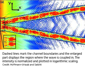
In the latest issue of Acta Crystallographica Section A: Foundations and Advances , Sarah Hoffmann-Urlaub and Tim Salditt report the fabrication and testing of a millimetre-sized chip capable of splitting a beam of X-rays. Fork-shaped channels that are only a few tens of nanometres wide and deep are transferred into a silicon wafer using electron-beam lithography and reactive ion etching then enclosed by bonding a second silicon wafer on top. The results of simulations of how the 'parent' beam is split into two 'daughter' beams on passing through the chip were backed up by experimental measurements at the European Synchrotron Radiation Facility, showing that the incident beam is efficiently transported through the chip, neatly split and guided to exits that have precisely controlled (and tunable) spacings. After the daughter beams leave the chip, they interfere, leading to a pattern of vertical stripes just like the pattern obtained from a classical Young's double-slit interference experiment. Interestingly, on close inspection there are fork-like structures within the stripes that originate from discontinuities in the phase of the recombined beam, forming striking features known as phase vortices. Furthermore, from those interference patterns the intensity distribution in the exit plane of the channels is reconstructed, which is found to be in very good agreement to the actual channel design.
This study complements earlier work on two-dimensionally confined channels in silicon in straight and tapered geometries, and paves the way to realizing `X-ray optics on a chip'. Illumination of samples by the two beams could provide some interesting advantages for coherent imaging and opens up the possibility of a new form of nano-interferometer. The authors envisage future development of their beamsplitter to create several daughter beams from the same parent beam, which would allow a single object to be imaged simultaneously by several beams, each from a different direction.
Share on:


Testimonial
"We’re proud to call I-Connect007 a trusted partner. Their innovative approach and industry insight made our podcast collaboration a success by connecting us with the right audience and delivering real results."
Julia McCaffrey - NCAB GroupSuggested Items
MEMS & Imaging Sensors Summit to Spotlight Sensing Revolution for Europe’s Leadership
09/11/2025 | SEMIIndustry experts will gather November 19-20 at the SEMI MEMS & Imaging Sensors Summit 2025 to explore the latest breakthroughs in AI-driven MEMS and imaging optimization, AR/VR technologies, and advanced sensor solutions for critical defence applications.
Direct Imaging System Market Size to Hit $4.30B by 2032, Driven by Increasing Demand for High-Precision PCB Manufacturing
09/11/2025 | Globe NewswireAccording to the SNS Insider, “The Direct Imaging System Market size was valued at $2.21 Billion in 2024 and is projected to reach $4.30 Billion by 2032, growing at a CAGR of 8.68% during 2025-2032.”
I-Connect007’s Editor’s Choice: Five Must-Reads for the Week
07/04/2025 | Marcy LaRont, I-Connect007For our industry, we have seen several bullish market announcements over the past few weeks, including one this week by IDC on the massive growth in the global server market. We’re also closely watching global trade and nearshoring. One good example of successful nearshoring is Rehm Thermal Systems, which celebrates its 10th anniversary in Mexico and the official opening of its new building in Guadalajara.
Driving Innovation: Direct Imaging vs. Conventional Exposure
07/01/2025 | Simon Khesin -- Column: Driving InnovationMy first camera used Kodak film. I even experimented with developing photos in the bathroom, though I usually dropped the film off at a Kodak center and received the prints two weeks later, only to discover that some images were out of focus or poorly framed. Today, every smartphone contains a high-quality camera capable of producing stunning images instantly.
United Electronics Corporation Advances Manufacturing Capabilities with Schmoll MDI-ST Imaging Equipment
06/24/2025 | United Electronics CorporationUnited Electronics Corporation has successfully installed the advanced Schmoll MDI-ST (XL) imaging equipment at their advanced printed circuit board facility. This significant technology investment represents a continued commitment to delivering superior products and maintaining their position as an industry leader in precision PCB manufacturing.