


 Dan’s Biz Bookshelf: Four Important Books You Need to Read (Not Just Say You Have)
 The Marketing Minute: Cracking the Code of Technical Marketing


New Theory Could Lead to New Generation of Energy Friendly Optoelectronics
August 22, 2016 | Queen’s University BelfastEstimated reading time: 1 minute
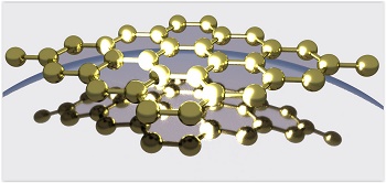
Researchers at Queen’s University Belfast and ETH Zurich, Switzerland, have created a new theoretical framework which could help physicists and device engineers design better optoelectronics, leading to less heat generation and power consumption in electronic devices which source, detect, and control light.
Speaking about the research, which enables scientists and engineers to quantify how transparent a 2D material is to an electrostatic field, Dr Elton Santos from the Atomistic Simulation Research Centre at Queen’s, said: “In our paper we have developed a theoretical framework that predicts and quantifies the degree of ‘transparency’ up to the limit of one-atom-thick, 2D materials, to an electrostatic field.
“Imagine we can change the transparency of a material just using an electric bias, e.g. get darker or brighter at will. What kind of implications would this have, for instance, in mobile phone technologies? This was the first question we asked ourselves. We realised that this would allow the microscopic control over the distribution of charged carriers in a bulk semiconductor (e.g. traditional Si microchips) in a nonlinear manner. This will help physicists and device engineers to design better quantum capacitors, an array of subatomic power storage components capable to keep high energy densities, for instance, in batteries, and vertical transistors, leading to next-generation optoelectronics with lower power consumption and dissipation of heat (cold devices), and better performance. In other words, smarter smart phones.”
Explaining how the theory could have important implications for future work in the area, Dr Santos added: “Our current model simply considers an interface formed between a layer of 2D material and a bulk semiconductor. In principle, our approach can be readily extended to a stack of multiple 2D materials, or namely, van der Waals heterostructures recently fabricated. This will allow us to design and predict the behaviour of these cutting-edge devices in prior to actual fabrication, which will significantly facilitate developments for a variety of applications. We will have an in silico search for the right combination of different 2D crystals while reducing the need for expensive lab work and test trials.”
Share on:


Testimonial
"We’re proud to call I-Connect007 a trusted partner. Their innovative approach and industry insight made our podcast collaboration a success by connecting us with the right audience and delivering real results."
Julia McCaffrey - NCAB GroupSuggested Items
Accelerating Embedded Innovation: Orthogone Becomes Texas Instruments Design Partner
09/17/2025 | PRNewswireOrthogone Technologies Inc., a leader in advanced embedded systems and FPGA development, is proud to announce its official designation as a Texas Instruments (TI) Design Services Partner.
BLT Joins Microchip Partner Program as Design Partner
09/17/2025 | BUSINESS WIREBLT, a U.S.-owned and operated engineering design services firm announced it has joined the Microchip Design Partner Program.
Staying on Top of Signal Integrity Challenges
09/16/2025 | Andy Shaughnessy, Design007 MagazineOver the years, Kris Moyer has taught a variety of advanced PCB design classes, both online IPC courses and in-person classes at California State University-Sacramento, where he earned his degrees in electrical engineering. Much of his advanced curriculum focuses on signal integrity, so we asked Kris to discuss the trends he’s seeing in signal integrity today, the SI challenges facing PCB designers, and his go-to techniques for controlling or completely eliminating SI problems.
American Standard Circuits to Exhibit and Host Lunch & Learn at PCB West 2025
09/17/2025 | American Standard CircuitsAnaya Vardya, President, and CEO of American Standard Circuits/ASC Sunstone Circuits has announced that his company will once again be exhibiting at PCB West 2025 to be held at the Santa Clara Convention Center on Wednesday, October 1, 2025.
ASM Technologies Limited signs MoU with the Guidance, Government of Tamilnadu to Expand Design-Led Manufacturing capabilities for ESDM
09/15/2025 | ASM TechnologiesASM Technologies Limited, a pioneer in Design- Led Manufacturing in the semiconductor and automotive industries, announced signing of Memorandum of Understanding (MoU) with the Guidance, Government of Tamilnadu whereby it will invest Rs. 250 crores in the state to expand its ESDM related Design-Led Manufacturing and precision engineering capacity. ASM Technologies will acquire 5 acres of land from the Government of Tamilnadu to set up a state-of-the-art design facility in Tamil Nadu's growing technology manufacturing ecosystem, providing a strong strategic advantage and long-term benefits for ASM.