


 Smart Automation: The Journey of a Component Through an SMT Factory
 Powering the Future: Why Thermal Management Defines the Future of Electronics
 Standard of Excellence: Engineering Is the New Sales—How Technical Collaboration Wins Business


Saki Demonstrates 3D AOI Systems at NEPCON South China
August 25, 2016 | Saki CorporationEstimated reading time: 1 minute
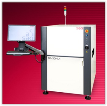
Saki Corporation will demonstrate its 2D and 3D automated optical inspection (AOI) systems at NEPCON South China in booth 1G35. Saki's AOI systems' unique Phase Measurement Profilometry technology and quad-directional side cameras inspect and measure QFNs, J-leads, and connectors, and enable the detection of the most difficult defects, such as lifted leads, tombstones, reverses, and height variations, without a reduction in speed. NEPCON South China is being held August 30-September 1, 2016 at the Shenzhen Convention & Exhibition Center, Shenzhen, China.
On display will be Saki's BF-3Di-L1, for L size boards, and BF-3Di-D1, with dual lanes. The systems measure heights from 0 to 20mm and from all four directions without a dead angle. They enable full automation with very low false calls and zero escapes. Failures of microchips with small pads and parts that have bottom electrodes are detected and the software directly reads sample and component height data to analyze assembly conditions.
Also on display will be Saki's BF-TristarII high-speed selective solder inspection and simultaneous two-sided inspection system. Two separate production processes can now be done in one simple process. It can inspect top-side SMT and bottom-side reflow or through-hole components on both sides in one pass, including inspection for stray parts. This compact machine can even be easily installed into a cell production line.
About Saki Corporation
Since its inception in 1994, Saki has led the way in the development of automatic recognition through robotic vision technology, applying ground-breaking image processing tools to solve inspection problems associated with printed circuit board assembly. Saki Corporation has headquarters in Tokyo, Japan with offices and sales and support centers around the world. Saki has Quality Management System JIS Q 9001:2008 and ISO 9001:2008 certifications.
Share on:


Testimonial
"Your magazines are a great platform for people to exchange knowledge. Thank you for the work that you do."
Simon Khesin - Schmoll MaschinenSuggested Items
ACCM Unveils Negative and Near-zero CTE Materials for Large-Format AI Chips
04/21/2026 | Advanced Chip and Circuit MaterialsAdvanced Chip and Circuit Materials, Inc. (ACCM) has launched two new materials: Celeritas HM50, with a negative coefficient of thermal expansion (CTE) of -8 ppm/°C to offset the positive CTE and expansion of copper with temperature on circuit boards, and Celeritas HM001, with near-zero CTE and the low-loss performance needed for high-speed signal layers to 224 Gb/s and faster in artificial intelligence (AI) circuits.
SMTA Ultra HDI Symposium, Day 2: Fragile Supply Chains, Fierce Innovation
04/14/2026 | Marcy LaRont, I-Connect007The Arizona weather yielded another beautiful day as we gathered for the second day of SMTA’s annual UHDI symposium. After the first full day discussing the role of AI in business and the how-tos of implementation, Avondale Mayor Mike Pineda kicked off day two, proud to showcase his city and to declare its important place in the continued development of the West Valley, an increasingly important area for tech and manufacturing.
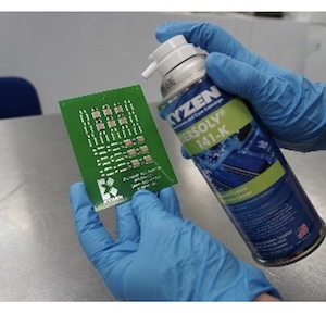
KYZEN Focuses on Aqueous and Stencil Cleaning Solutions at SMTA Monterrey Expo and Tech Forum
04/10/2026 | KYZEN'KYZEN, the global leader in innovative environmentally friendly cleaning chemistries, will exhibit at the SMTA Monterrey Expo & Tech Forum.
Solder Paste Innovations for Enhanced Reliability from MacDermid Alpha Electronics Solutions
04/10/2026 | Real Time with... APEX EXPOJason Fullerton of MacDermid Alpha Electronics Solutions discusses innovative alloys like Innolot MXE, low-temperature solder options, and polymer reinforcement strategies. Learn how these solutions address the growing demands of high-performance computing and larger component assemblies, ensuring optimal performance and cost-effectiveness.
Frank Sommer Discusses Selective Soldering Innovations for EVs
04/10/2026 | Real Time with... APEX EXPODan Beaulieu sits down with Frank Sommer, a selective soldering expert from Nordson Electronics Solutions, to discuss the resurgence of selective soldering driven by electric vehicle manufacturing, and the need for robust through-hole component integration. He also introduces Nordson's innovative SELECT Synchro selective soldering machine, designed for enhanced throughput and flexibility.