


 Dan’s Biz Bookshelf: Four Important Books You Need to Read (Not Just Say You Have)
 The Marketing Minute: Cracking the Code of Technical Marketing


Low-cost and Defect-free Graphene
September 8, 2016 | FAUEstimated reading time: 2 minutes
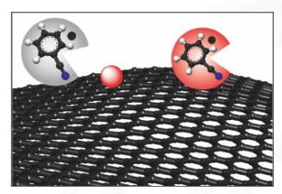
Graphene is one of the most promising new materials. However, researchers across the globe are still looking for a way to produce defect-free graphene at low costs. Chemists at Friedrich-Alexander-Universiät Erlangen-Nürnberg (FAU) have now succeeded in producing defect-free graphene directly from graphite for the first time.
Graphene is two dimensional and consists of a single layer of carbon atoms. It is particularly good at conducting electricity and heat, transparent and flexible yet strong. Graphene's unique properties make it suitable for use in a wide range of pioneering technologies, such as in transparent electrodes for flexible displays.
However, the semi-conductor industry will only be able to use graphene successfully once properties such as the size, area and number of defects - which influence its conductivity - can be improved during synthesis. A team of FAU researchers led by Dr. Andreas Hirsch from the Chair of Organic Chemistry II has recently made a crucial break-through in this area. With the help of the additive benzonitrile, they have found a way of producing defect-free graphene directly from a solution. Their method enables the graphene - which is of a higher quality than ever achieved before - to be cut without causing defects and also allows specific electronic properties to be set through the number of charge carriers. Furthermore, their technique is both low-cost and efficient.
A common way of synthesising graphene is through chemical exfoliation of graphite. In this process, metal ions are embedded in graphite, which is made of carbon, resulting in what is known as an intercalation compound. The individual layers of carbon - the graphene - are separated using solvents. The stabilised graphene then has to be separated from the solvent and reoxidised. However, defects in the individual layers of carbon, such as hydration and oxidation of carbon atoms in the lattice, can occur during this process. FAU researchers have now found a solution to this problem. By adding the solvent benzonitrile, the graphene can be removed without any additional functional groups forming - and it remains defect-free.
'This discovery is a break-through for experts in the international field of reductive graphene synthesis,' Professor Hirsch explains. 'Based on this discovery we can expect to see major advancements in terms of the applications of this type of graphene which is produced using wet chemical exfoliation. An example could be cutting defect-free graphene for semi-conductor or sensor technology.'
Additional benefits
The method devised by FAU researchers has another advantage: the reduced benzonitrile molecule formed during the reaction turns red as long as it does not come into contact with oxygen or water. This change in colour allows the number of charge carriers in the system to be determined easily through absorption measurements. This could previously only be done by measuring voltage and means that graphene and battery researchers now have a new way of measuring the charge state.
Share on:


Testimonial
"The I-Connect007 team is outstanding—kind, responsive, and a true marketing partner. Their design team created fresh, eye-catching ads, and their editorial support polished our content to let our brand shine. Thank you all! "
Sweeney Ng - CEE PCBSuggested Items
Rules of Thumb: Design007 Magazine, November 2024
11/11/2024 | I-Connect007 Editorial TeamRules of thumb are everywhere, but there may be hundreds of rules of thumb for PCB design. They’re built on design formulas, fabricators’ limitations, and tribal knowledge. And unfortunately, some longtime rules of thumb should be avoided at all costs. How do we separate the wheat from the chaff, so to speak?
Connect the Dots: Best Practices for Prototyping
09/21/2023 | Matt Stevenson -- Column: Connect the DotsPCB prototyping is a critical juncture during an electronic device’s journey from concept to reality. Regardless of a project’s complexity, the process of transforming a design into a working board is often enlightening in terms of how a design can be improved before a PCB is ready for full production.
The Drive Toward UHDI and Substrates
09/20/2023 | I-Connect007 Editorial TeamPanasonic’s Darren Hitchcock spoke with the I-Connect007 Editorial Team on the complexities of moving toward ultra HDI manufacturing. As we learn in this conversation, the number of shifting constraints relative to traditional PCB fabrication is quite large and can sometimes conflict with each other.
Asia/Pacific AI Spending Surge to Reach a Projected $78 Billion by 2027
09/19/2023 | IDCAsia/Pacific spending on Artificial Intelligence (AI) ), including software, services, and hardware for AI-centric systems will grow to $78.4 billion in 2027, according to International Data Corporation's latest Worldwide Artificial Intelligence Spending Guide.
Intel to Sell Minority Stake in IMS Nanofabrication Business to TSMC
09/13/2023 | IntelIntel Corporation announced that it has agreed to sell an approximately 10% stake in the IMS Nanofabrication business to TSMC. TSMC’s investment values IMS at approximately $4.3 billion, consistent with the valuation of the recent stake sale to Bain Capital Special Situations.