


 The Chemical Connection: Onshoring PCB Production—Daunting but Certainly Possible
 It’s Only Common Sense: The Phone Is Still Mightier Than the Keyboard


Squeezing Light Into New Miniature Devices
November 28, 2016 | Institute for Basic ScienceEstimated reading time: 2 minutes
Do you think your computer is fast enough? Think again. The computers of the future could work almost at the speed of light! Nanophotonics, the study of light at the nanometer scale, could indeed bring the speed of our technology to a completely different level.
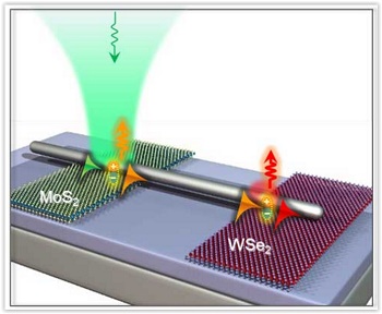
The multiplexer device with one input and two outputs. The plus-minus couple indicates the exciton.
The Center for Integrated Nanostructure Physics (CINAP) within the Institute for Basic Science (IBS) have developed three key components of a circuit that works with light. Published in Nature Communications ("Reconfigurable exciton-plasmon interconversion for nanophotonic circuits"), these devices combine the advantages of photonics and electronics on the same platform.
While we are slowing approaching the end point of Moore's Law: a state where we physically cannot shrink the dimension of our transistors much further; the future of big data processing requires high performance computers with higher speed operations. Researchers reckon that if we build computers that process information through light, instead of electrons, computer will be able to work faster.
However, at nanometer dimensions, the wavelength of light is larger than the diameter of the silicon fiber and for this reason some light can be lost. A solution to control the propagation of light in matter can come from surface plasmons. These are electromagnetic waves that propagate along the surface of some conductive materials like silver, gold, aluminum and copper. Using surface plasmons, optical information can be transmitted nearly at the speed of light and in extremely miniature volumes.
Using surface plasmons in silver nanowires and 2D semiconductors like molybdenum disulphide (MoS2), IBS scientists built three key components for optical communication: optical transistors, optical multiplexers and optical signal detectors.
These devices work thanks to a phenomenon called plasmon-exciton-plasmon interconversion. The graphics describe the details of this process step-by-step.
IBS scientists constructed the optical transistor by interconnecting the silver nanowire to a flake of MoS2. Light shone on the device is converted to surface plasmon, than to exciton, back to surface plasmon and eventually emitted as light with a shorter wavelength compared to the initial input. For example, if the input light is green, the output light can be red.
Wavelength multiplexing devices were realized in a similar way, but instead of having only a flake of MoS2, the researchers used an array of three different 2D semiconductor materials emitting light at different wavelengths. In this structure, for example, a single input light (violet color) generates three output lights (blue, green and red).
The propagating optical signals along the silver nanowire can be also transformed and detected as electrical signals by an optical signal detector.
“The originality of this paper arises from the exciton-plasmon interconversion. We published before the conversion of exciton to plasmon, and from plasmon to exciton using silver nanowire/2D semiconductor hybrids, but this is the first time that we can complete the circle going from plasmons to excitons and back to plasmons. Using this concept, we created optical transistors and multiplexors,” explains professor Hyun Seok Lee, first author of this study.
Share on:


Testimonial
"The I-Connect007 team is outstanding—kind, responsive, and a true marketing partner. Their design team created fresh, eye-catching ads, and their editorial support polished our content to let our brand shine. Thank you all! "
Sweeney Ng - CEE PCBSuggested Items
Episode 6 of Ultra HDI Podcast Series Explores Copper-filled Microvias in Advanced PCB Design and Fabrication
10/15/2025 | I-Connect007I-Connect007 has released Episode 6 of its acclaimed On the Line with... American Standard Circuits: Ultra High Density Interconnect (UHDI) podcast series. In this episode, “Copper Filling of Vias,” host Nolan Johnson once again welcomes John Johnson, Director of Quality and Advanced Technology at American Standard Circuits, for a deep dive into the pros and cons of copper plating microvias—from both the fabricator’s and designer’s perspectives.
Nolan’s Notes: Tariffs, Technologies, and Optimization
10/01/2025 | Nolan Johnson -- Column: Nolan's NotesLast month, SMT007 Magazine spotlighted India, and boy, did we pick a good time to do so. Tariff and trade news involving India was breaking like a storm surge. The U.S. tariffs shifted India from one of the most favorable trade agreements to the least favorable. Electronics continue to be exempt for the time being, but lest you think that we’re free and clear because we manufacture electronics, steel and aluminum are specifically called out at the 50% tariff levels.
MacDermid Alpha & Graphic PLC Lead UK’s First Horizontal Electroless Copper Installation
09/30/2025 | MacDermid Alpha & Graphic PLCMacDermid Alpha Electronics Solutions, a leading supplier of integrated materials and chemistries to the electronics industry, is proud to support Graphic PLC, a Somacis company, with the installation of the first horizontal electroless copper metallization process in the UK.
Electrodeposited Copper Foils Market to Grow by $11.7 Billion Over 2025-2032
09/18/2025 | Globe NewswireThe global electrodeposited copper foils market is poised for dynamic growth, driven by the rising adoption in advanced electronics and renewable energy storage solutions.
MacDermid Alpha Showcases Advanced Interconnect Solutions at PCIM Asia 2025
09/18/2025 | MacDermid Alpha Electronics SolutionsMacDermid Alpha Electronic Solutions, a global leader in materials for power electronics and semiconductor assembly, will showcase its latest interconnect innovations in electronic interconnect materials at PCIM Asia 2025, held from September 24 to 26 at the Shanghai New International Expo Centre, Booth N5-E30