


 It’s Only Common Sense: Your Biggest Competitor Is Complacency
 The Chemical Connection: Onshoring PCB Production—Daunting but Certainly Possible


The Future is Flat (For Lenses)
January 9, 2017 | CaltechEstimated reading time: 2 minutes
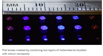
Engineers at Caltech have developed a system of flat optical lenses that can be easily mass-produced and integrated with image sensors, paving the way for cheaper and lighter cameras in everything from cell phones to medical devices.
The technology relies on stacking two metasurfaces. Metasurfaces are sheets of material whose electromagnetic properties can be altered on demand. In this case, the metasurfaces are dotted with silicon cylinders smaller than a micron across that alter the way light passes through them.
"The way we make lenses hasn't changed much since the time of van Leeuwenhoek. Until now," says Caltech's Andrei Faraon (BS '04), referring to Antonie van Leeuwenhoek, a Dutch scientist and lens-maker who created some of the first microscopes.
Faraon, assistant professor of applied physics and materials science in Caltech's Division of Engineering and Applied Science, collaborated with Caltech postdoctoral researcher Amir Arbabi and Seunghoon Han from Samsung Electronics to develop the lens system. Their work was published in Nature Communications on November 28.
A classical lens made of plastic or glass has a curved shape that bends the path of incoming light toward a single focal point. This is because light travels faster through the thinner glass at the edges of the lens than through the thicker glass at the center.
The metasurfaces accomplish the same task using silicon nanoposts, cylinders just 600 nanometers tall and with varying diameters in the hundreds of nanometers. (For scale, a strand of human hair is 100,000 nanometers wide.) Each metasurface is dotted with tens of millions of these posts. Light travels faster through nanoposts with smaller diameters than through nanoposts with larger diameters, so controlling the width of the nanoposts allows the engineers to finely adjust the path of light passing through the metasurface to create flat lenses.
Early experiments with nanopost metasurfaces yielded lenses whose images were blurry around the edges—like a magnifying glass. However, by coupling two metasurfaces together, each nanopost-side-out, the engineers were able to create a lens system that can capture and focus light from a 70-degree angular range, making the technology useful for the first time in microscope and camera imaging applications.
"Metasurfaces like these can be easily mass produced, much the way computer chips are," Arbabi says. "That means this could be a cheap and easily scalable way to create tiny lenses just a few millimeters in diameter."
In addition, the lenses can be seamlessly integrated with CMOS (complementary metal-oxide semiconductor) image sensors because they are made using the same materials and fabrication techniques. CMOS image sensors are the tiny chips that underpin digital photography, and were developed at JPL.
Flat, lightweight, and cheap lenses are in demand for various consumer electronics equipped with cameras, or medical devices such as endoscopes, Faraon says.
Next, the team plans to integrate these lenses into miniaturized cameras and microscopes, and extend their functionality and operation bandwidth.
Share on:


Testimonial
"In a year when every marketing dollar mattered, I chose to keep I-Connect007 in our 2025 plan. Their commitment to high-quality, insightful content aligns with Koh Young’s values and helps readers navigate a changing industry. "
Brent Fischthal - Koh YoungSuggested Items
How PCBA Excellence Transforms High-mix Operations
09/22/2025 | Chintan Sanghani, Electronics Center for ExcellenceWith over 30 years of manufacturing excellence, our organization has built deep expertise in PCBA contract manufacturing for downhole oilfield tools. Through years of focused operational leadership in this demanding sector, we've learned that in high-mix, low-volume (HMLV) environments, traditional manufacturing approaches can create more bottlenecks than breakthroughs.
Advint Incorporated Brings Artificial Intelligence to Electroplating Training
09/11/2025 | Advint IncorporatedAdvint Incorporated is introducing a new dimension to its electroplating training programs: the integration of Artificial Intelligence (AI). This initiative reflects the company’s commitment to providing PCB fabricators and manufacturers in the USA and Canada with training that is practical, forward-looking, and directly relevant to today’s production challenges.
The Signal Integrity Issue: Design007 Magazine September 2025
09/09/2025 | I-Connect007 Editorial TeamAs the saying goes, “If you don’t have signal integrity problems now, you will eventually.” This month, our experts share a variety of design techniques that can help PCB designers and design engineers achieve signal integrity.
Semiconductors Get Magnetic Boost with New Method from UCLA Researchers
07/31/2025 | UCLA NewsroomA new method for combining magnetic elements with semiconductors — which are vital materials for computers and other electronic devices — was unveiled by a research team led by the California NanoSystems Institute at UCLA.
SMT Perspectives and Prospects: Warren Buffett’s Perpetual Wisdom, Part 1
07/29/2025 | Dr. Jennie Hwang -- Column: SMT Perspectives and ProspectsOver the years, I have cherished the lessons by Warren Buffett and Charlie Munger at the Berkshire Hathaway annual shareholders meeting in Omaha, Nebraska. This year, I was among the more than 40,000 who attended the May 3 meeting. Millions more from around the world, including from the UK, Germany, Japan, China, Panama, and Guatemala, tuned in remotely and via CNBC’s livestream.