


 Global PCB Connections: Rigid-flex and Flexible PCBs—The Backbone of Modern Electronics
 Flexible Thinking: The Key to a Successful Flex Circuit Design Transfer
 Happy’s Tech Talk #29: Bend-to-Install Semi-flex FR-4


Panasonic Commercializes Low Transmission Loss Flexible Multi-layer Circuit Board Materials
January 17, 2017 | Panasonic CorporationEstimated reading time: 4 minutes
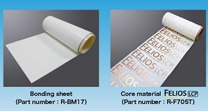
Panasonic Corporation announced today that it has commercialized its Low Transmission Loss[1] Flexible Multi-layer Circuit Board Materials, suitable for high-speed large-volume data transmission and thinner designs of mobile devices, including smartphones and tablet computers. The company will launch its mass production in January 2017. The combination of a liquid-crystal polymer (LCP) core material[2] and a bonding sheet material that can be laminated at a low temperature and stored at room temperature will considerably ease the manufacture of high-frequency flexible multi-layer circuit boards.
Existing coaxial cables used for large-volume transmission are thick, so they present an obstacle to making mobile devices thinner. Low transmission loss flexible multi-layer circuit boards are of increasing potential as a solution that achieves both large-volume data transmission and a thin design, but they face many restrictions in how they should be handled, due to the characteristics of the materials they incorporate, so they require special facilities for manufacturing. Using its unique resin design technologies, Panasonic has developed a bonding sheet that can be laminated at a low temperature of less than 200 °C and stored at room temperature. This eliminates the need for special facilities for high-temperature lamination and refrigerated storage for bonding sheets. The company has also achieved high adhesiveness of LCP and low profile copper foil for the LCP core material by using its unique laminating techniques. Although existing flexible core materials using polyimide and so on are usable for only low-speed transmission, the new material, due to its low transmission loss property can also be used for high-speed transmission of large-volume data.
Panasonic's new flexible multi-layer circuit board materials have the following features:
- Low transmission loss and compatibility with USB 3.1 Gen 2 (10 Gbps) enable the transmission of large-volume data at higher speeds
- Transmission loss: -2 dB/100 mm @ 6 GHz*1.
- Core material: Dielectric constant: 2.9 @ 10 GHz, dissipation factor: 0.002 @ 10 GHz
- Bonding sheet: Dielectric constant: 2.2 @ 10 GHz, dissipation factor: 0.001 @ 10 GHz
- Flexible multi-layer circuit board adopts a 3-layer structure with multiple of signal lines at a thickness of 0.2 mm, allowing further thinning of mobile devices.
- Total board thickness: 0.2 mm or less(1)
- Circuit board material that can be laminated at a low temperature and stored at room temperature makes manufacturing of flexible multi-layer circuit boards easier.
- Lamination temperature: 180 - 200°C, existing bonding sheet(2): 300°C
- Room-temperature storage: 23 (±5) °C, existing bonding sheet(3): refrigerated storage: 5°C or below
(2) Panasonic's conventional LCP bonding sheet
(3) Ordinary low-dielectric constant bonding sheet
Suitable applications:
Circuit boards for high-frequency antenna modules, high-speed cables, etc.
Panasonic Technology
1. Low transmission loss and compatibility with USB 3.1 Gen 2 (10 Gbps) contribute to transmission of large-volume data at higher speeds
There is a growing need for faster transmission of signals due to the increasing volume of data demanded by the ever-higher resolutions of mobile device cameras and display screens. As a result, low transmission loss flexible multi-layer circuit boards that enable large-volume, high-speed transmission are of increasing interest as a replacement for currently-used coaxial cables; and low transmission loss, meaning that only a small amount of the signal is lost during transmission, is desired for the circuit board material. Panasonic has commercialized a low transmission loss core material and bonding sheet by applying its unique resin design technologies. It supports standards including USB 3.1 Gen 2 (10 Gbps) and will enable increased speed of large-volume data transmission in mobile devices.
2. Flexible multi-layer circuit board comprising a 3-layer, 0.2 mm-thick structure with multiple signal lines contributes to thinner mobile device designs
A coaxial cable is composed of one signal line in a cable and is capable of large-volume data transmission, but its downside is its thickness. A low transmission loss flexible multi-layer circuit board has several signal lines within it, so large-volume data transmission and a thinner design can be achieved simultaneously. Adopting this material allows flexible multi-layer circuit boards, in a 0.2 mm-thick, 3-layer structure that can carry several signal lines, to replace coaxial cables.
3. Circuit board material that can be laminated at a low temperature and stored at room temperature facilitates the manufacture of flexible multi-layer circuit boards
Previous bonding sheet, which forms the low transmission loss flexible multi-layer circuit boards with core material, had to be laminated at a high temperature or stored refrigerated. It was also difficult to handle, due to its material characteristics, and required special facilities that placed a burden on manufacturers. Using its unique resin design technologies, Panasonic has developed a bonding sheet that can be laminated at a low temperature of 200 °C or less, and stored at room temperature, making it far easier to handle the material during production. By providing this sheet and the low-transmission loss core material, the company will considerably facilitate the production of flexible multi-layer circuit boards.
Basic specifications
About Panasonic
Panasonic Corporation is a worldwide leader in the development of diverse electronics technologies and solutions for customers in the consumer electronics, housing, automotive, enterprise solutions and device industries. Since its founding in 1918, the company has expanded globally and now operates 474 subsidiaries and 94 associated companies worldwide, recording consolidated net sales of 7.553 trillion yen for the year ended March 31, 2016. Committed to pursuing new value through innovation across divisional lines, the company uses its technologies to create a better life and a better world for its customers. To learn more about Panasonic, click here.
Share on:


Testimonial
"The I-Connect007 team is outstanding—kind, responsive, and a true marketing partner. Their design team created fresh, eye-catching ads, and their editorial support polished our content to let our brand shine. Thank you all! "
Sweeney Ng - CEE PCBSuggested Items
Episode 6 of Ultra HDI Podcast Series Explores Copper-filled Microvias in Advanced PCB Design and Fabrication
10/15/2025 | I-Connect007I-Connect007 has released Episode 6 of its acclaimed On the Line with... American Standard Circuits: Ultra High Density Interconnect (UHDI) podcast series. In this episode, “Copper Filling of Vias,” host Nolan Johnson once again welcomes John Johnson, Director of Quality and Advanced Technology at American Standard Circuits, for a deep dive into the pros and cons of copper plating microvias—from both the fabricator’s and designer’s perspectives.
Nolan’s Notes: Tariffs, Technologies, and Optimization
10/01/2025 | Nolan Johnson -- Column: Nolan's NotesLast month, SMT007 Magazine spotlighted India, and boy, did we pick a good time to do so. Tariff and trade news involving India was breaking like a storm surge. The U.S. tariffs shifted India from one of the most favorable trade agreements to the least favorable. Electronics continue to be exempt for the time being, but lest you think that we’re free and clear because we manufacture electronics, steel and aluminum are specifically called out at the 50% tariff levels.
MacDermid Alpha & Graphic PLC Lead UK’s First Horizontal Electroless Copper Installation
09/30/2025 | MacDermid Alpha & Graphic PLCMacDermid Alpha Electronics Solutions, a leading supplier of integrated materials and chemistries to the electronics industry, is proud to support Graphic PLC, a Somacis company, with the installation of the first horizontal electroless copper metallization process in the UK.
Electrodeposited Copper Foils Market to Grow by $11.7 Billion Over 2025-2032
09/18/2025 | Globe NewswireThe global electrodeposited copper foils market is poised for dynamic growth, driven by the rising adoption in advanced electronics and renewable energy storage solutions.
MacDermid Alpha Showcases Advanced Interconnect Solutions at PCIM Asia 2025
09/18/2025 | MacDermid Alpha Electronics SolutionsMacDermid Alpha Electronic Solutions, a global leader in materials for power electronics and semiconductor assembly, will showcase its latest interconnect innovations in electronic interconnect materials at PCIM Asia 2025, held from September 24 to 26 at the Shanghai New International Expo Centre, Booth N5-E30