


 Dan’s Biz Bookshelf: ‘The Next RenAIssance: AI and the Expansion of Human Potential’
 The Chemical Connection: When the Industry Moves Faster Than the Standards
 Driving Innovation: Selecting the Right Laser Source


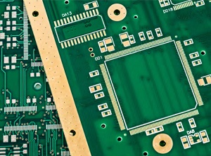
Study of Immersion Gold Processes Used for Both ENIG & ENEPIG
February 1, 2017 | Don Gudeczauskas, Albin Gruenwald and George Milad, Uyemura International CorporationEstimated reading time: 2 minutes
Abstract
The use of electroless nickel/electroless palladium/immersion gold (ENEPIG) has been steadily increasing the past several years and benefits of the finish have now become well-known throughout the industry. The finish provides both reliable solder joints and wire bonds.
In some Asian countries where mass production is performed at many facilities, dedicated production lines have been installed for plating of ENEPIG using an immersion gold optimized for ENEPIG but not for electroless nickel/immersion gold (ENIG). In the North American market, however, many PWB facilities are producing both ENIG and ENEPIG finishes from the same plating line due to lower overall production volumes and desire to use the same immersion gold for both finishes. Most facilities have neither the room for two separate immersion golds nor the desire to tie up capital with the cost of gold for two separate immersion gold tanks.
The challenge for North American manufacturers has been in choosing the proper immersion gold chemistry which can suitably deposit gold for ENIG and ENEPIG while providing a robust finish for soldering, wire bonding, and electrical contact with both finishes.
This paper presents results of a comparative study on three types of immersion golds which could be used for both ENIG and ENEPIG deposits in the same production line: standard displacement immersion gold, high efficiency immersion gold which limits nickel dissolution, and a mixed reaction immersion gold which utilizes a mild reducing agent. Comparative results for solder wetting force, solder joint reliability and wire bonding will be presented for ENEPIG. Additionally, plated samples will be examined by SEM for evidence of nickel or palladium damage from the immersion gold plating operation.
Introduction
Recently, it is well-known that the electroless ENEPIG process has excellent solder joint reliability (SJR) and that it has the same wire bond reliability (WBR) compared to electroless Ni/Au with thicker Au (ENAG) process, even if the electroless Au thickness is between 0.1 to 0.2µm. Past studies have examined the performance of ENEPIG[1,2]. The current IPC ENEPIG specification (IPC-4554 Amendment 1) calls for gold thicknesses between 1.2 µin minimum at 4 sigma below the mean and 2.8 µin maximum, and some specific customer requirements call for even thicker gold. It has been found that thicker deposits of immersion gold might lead to nickel corrosion with ENEPIG if the dwell time in the immersion gold solution is too long.
The goal of this study was to examine the performance of ENEPIG using three different types of immersion gold: standard displacement immersion gold, high efficiency immersion gold, and reduction assisted immersion gold.
The three types of immersion gold dissolve corresponding different amounts of nickel while the gold deposits as shown in Figure 1 using ENIG. The high efficiency immersion gold dissolves approximately half the amount of nickel from that of the standard displacement immersion gold while the reduction assisted gold dissolves approximately 60 percent of the nickel dissolved from the high efficiency immersion gold solution. Later studies will compare results for these immersion golds with ENIG only.
Examination methods in this study included solder wetting balance tests, gold sire bonding tests, cross section analysis for nickel corrosion examination and for intermetallic formation after solder testing.
To read the full version of this article which appeared in the January 2017 issue of The PCB Magazine, click here.
Share on:


Testimonial
"We’re proud to call I-Connect007 a trusted partner. Their innovative approach and industry insight made our podcast collaboration a success by connecting us with the right audience and delivering real results."
Julia McCaffrey - NCAB GroupSuggested Items
Indium to Showcase High-Performance AI Application Solutions at SEMICON SEA 2026
05/01/2026 | Indium CorporationAs a leading provider of advanced materials solutions for today’s demanding AI applications, Indium Corporation® will feature its high-reliability product portfolio at SEMICON SEA 2026, May 5-7, in Kuala Lumpur, Malaysia.
ACCM Unveils Negative and Near-zero CTE Materials for Large-Format AI Chips
04/21/2026 | Advanced Chip and Circuit MaterialsAdvanced Chip and Circuit Materials, Inc. (ACCM) has launched two new materials: Celeritas HM50, with a negative coefficient of thermal expansion (CTE) of -8 ppm/°C to offset the positive CTE and expansion of copper with temperature on circuit boards, and Celeritas HM001, with near-zero CTE and the low-loss performance needed for high-speed signal layers to 224 Gb/s and faster in artificial intelligence (AI) circuits.
SMTA Ultra HDI Symposium, Day 2: Fragile Supply Chains, Fierce Innovation
04/14/2026 | Marcy LaRont, I-Connect007The Arizona weather yielded another beautiful day as we gathered for the second day of SMTA’s annual UHDI symposium. After the first full day discussing the role of AI in business and the how-tos of implementation, Avondale Mayor Mike Pineda kicked off day two, proud to showcase his city and to declare its important place in the continued development of the West Valley, an increasingly important area for tech and manufacturing.
KYZEN Focuses on Aqueous and Stencil Cleaning Solutions at SMTA Monterrey Expo and Tech Forum
04/10/2026 | KYZEN'KYZEN, the global leader in innovative environmentally friendly cleaning chemistries, will exhibit at the SMTA Monterrey Expo & Tech Forum.
Solder Paste Innovations for Enhanced Reliability from MacDermid Alpha Electronics Solutions
04/10/2026 | Real Time with... APEX EXPOJason Fullerton of MacDermid Alpha Electronics Solutions discusses innovative alloys like Innolot MXE, low-temperature solder options, and polymer reinforcement strategies. Learn how these solutions address the growing demands of high-performance computing and larger component assemblies, ensuring optimal performance and cost-effectiveness.