


 It’s Only Common Sense: If You’re Not Differentiated, You’re Dead
 Alpha Insights, Performance by Design: The Future of PCB Manufacturing in the Midwest
 Happy’s Tech Talk #43: Engineering Statistics Training With Free Software


Coffee-Ring Effect Leads to Crystallization Control in Semiconductors
March 9, 2017 | KAUSTEstimated reading time: 2 minutes
A chance observation of crystals forming a mark that resembled the stain of a coffee cup left on a table has led to the growth of customized polycrystals with implications for faster and more versatile semiconductors.
Thin-film semiconductors are the foundation of a vast array of electronic and optoelectronic devices. They are generally fabricated by crystallization processes that yield polycrystals with a chaotic mix of individual crystals of different orientations and sizes.
Significant advances in controlling crystallization has been made by a team led by Professor Aram Amassian of Material Science and Engineering at KAUST. The group included individuals from the KAUST Solar Center and others from the University’s Physical Science and Engineering Division in collaboration with Cornell University. Amassian said, “There is no longer a need to settle for random and incoherent crystallization.”
The team’s recent discovery began when Dr. Liyang Yu of the KAUST team noticed that a droplet of liquid semiconductor material dried to form an outer coffee-ring shape that was much thicker than the material at the center. When he induced the material to crystallize, the outer ring crystallized first.
“This hinted that local thickness matters for initiating crystallization,” said Amassian, which went against the prevailing understanding of how polycrystal films form.
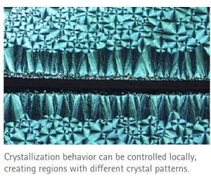
This anomaly led the researchers to delve deeper. They found that the thickness of the crystallizing film could be used to manipulate the crystallization of many materials (see top image). Most crucially, tinkering with the thickness also allowed fine control over the position and orientation of the crystals in different regions of a semiconductor.
“We discovered how to achieve excellent semiconductor properties everywhere in a polycrystal film,” said Amassian. He explained that seeding different patterns of crystallization at different locations also allowed the researchers to create bespoke arrays that can now be used in electronic circuits.
This is a huge improvement to the conventional practice of making do with materials whose good properties are not sustained throughout the entire polycrystal nor whose functions at different regions can be controlled.
“We can now make customized polycrystals on demand,” Amassian said.
Amassian hopes that this development will lead to high-quality, tailored polycrystal semiconductors to promote advances in optoelectronics, photovoltaics and printed electronic components. The method has the potential to bring more efficient consumer electronic devices, some with flexible and lightweight parts, new solar power generating systems and advances in medical electronics. And all thanks to the chance observation of an odd pattern in a semiconductor droplet.
The team will now explore ways to move their work beyond the laboratory through industry partnerships and research collaborations.
Share on:


Testimonial
"In a year when every marketing dollar mattered, I chose to keep I-Connect007 in our 2025 plan. Their commitment to high-quality, insightful content aligns with Koh Young’s values and helps readers navigate a changing industry. "
Brent Fischthal - Koh YoungSuggested Items
Advanced Semiconductor Packaging Market Sees Rising Adoption Across Automotive and Industrial Sectors
10/14/2025 | openPRThe semiconductor packaging market size is estimated to reach at a CAGR of 7.2% during the forecast period (2024-2031).
Imec Launches 300mm GaN Program to Develop Advanced Power Devices and Reduce Manufacturing Costs
10/13/2025 | ImecImec, a world-leading research and innovation hub in nanoelectronics and digital technologies, welcomes AIXTRON, GlobalFoundries, KLA Corporation, Synopsys, and Veeco as first partners in its 300mm gallium-nitride (GaN) open innovation program track for low- and high-voltage power electronics applications.
NEDME Returns October 22 — The Northwest’s Premier Design & Manufacturing Expo
10/13/2025 | NEDMEThe Northwest Electronics Design & Manufacturing Expo (NEDME) returns on Wednesday, October 22, 2025, at Wingspan Event & Conference Center, Hillsboro. The event brings together engineers, product designers, manufacturers, educators, and community partners for a full day of industry connection, learning, and networking.
L3Harris Announces New Variants of its VAMPIRE System
10/13/2025 | L3Harris TechnologiesL3Harris Technologies has expanded its VAMPIRE™ system, demonstrating the company’s ability to swiftly respond to the U.S. Department of War and allied partners’ urgent need to defeat small unmanned autonomous systems accurately and affordably.
Critical Minerals: The New Power Play in Global Trade
10/13/2025 | Marcy LaRont, I-Connect007Access to critical minerals essential for electronics manufacturing, and China’s monopoly of them, is increasingly under scrutiny, with gallium (Ga) and germanium (Ge)at the forefront of this discourse. However, all critical minerals imported from China share a similar narrative, and understanding the implications of this dependency and the risks to both U.S. commercial and defense sectors has created an urgent need for a comprehensive electronics strategy to secure and diversify access to these vital minerals. In this candid interview, USPAE Executive Director Jim Will discusses the issues and the mitigation steps that must be taken to adequately address them.