


 It’s Only Common Sense: Creativity Is Noisy, Messy, and So Worth It
 Dan’s Biz Bookshelf: ‘The Soul of a New Machine’
 The Chemical Connection: Back to Basic Cupric Chloride Etching


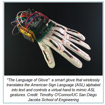
Engineers at the University of California San Diego have developed a smart glove that wirelessly translates the American Sign Language alphabet into text and controls a virtual hand to mimic sign language gestures. The device, which engineers call “The Language of Glove,” was built for less than $100 using stretchable and printable electronics that are inexpensive, commercially available and easy to assemble. The work was published on July 12 in the journal PLOS ONE.
In addition to decoding American Sign Language gestures, researchers are developing the glove to be used in a variety of other applications ranging from virtual and augmented reality to telesurgery, technical training and defense.
“Gesture recognition is just one demonstration of this glove’s capabilities,” said Timothy O’Connor, a nanoengineering Ph.D. student at UC San Diego and the first author of the study. “Our ultimate goal is to make this a smart glove that in the future will allow people to use their hands in virtual reality, which is much more intuitive than using a joystick and other existing controllers. This could be better for games and entertainment, but more importantly for virtual training procedures in medicine, for example, where it would be advantageous to actually simulate the use of one’s hands.”
The glove is unique in that it has sensors made from stretchable materials, is inexpensive and simple to manufacture. “We’ve innovated a low-cost and straightforward design for smart wearable devices using off-the-shelf components. Our work could enable other researchers to develop similar technologies without requiring costly materials or complex fabrication methods,” said Darren Lipomi, a nanoengineering professor who is a member of the Center for Wearable Sensors at UC San Diego and the study’s senior author.
The ‘Language of Glove’
The team built the device using a leather athletic glove and adhered nine stretchable sensors to the back at the knuckles — two on each finger and one on the thumb. The sensors are made of thin strips of a silicon-based polymer coated with a conductive carbon paint. The sensors are secured onto the glove with copper tape. Stainless steel thread connects each of the sensors to a low power, custom-made printed circuit board that’s attached to the back of the wrist.
The sensors change their electrical resistance when stretched or bent. This allows them to code for different letters of the American Sign Language alphabet based on the positions of all nine knuckles. A straight or relaxed knuckle is encoded as “0” and a bent knuckle is encoded as “1”. When signing a particular letter, the glove creates a nine-digit binary key that translates into that letter. For example, the code for the letter “A” (thumb straight, all other fingers curled) is “011111111,” while the code for “B” (thumb bent, all other fingers straight) is “100000000.” Engineers equipped the glove with an accelerometer and pressure sensor to distinguish between letters like “I” and “J”, whose gestures are different but generate the same nine-digit code.
The low power printed circuit board on the glove converts the nine-digit key into a letter and then transmits the signals via Bluetooth to a smartphone or computer screen. The glove can wirelessly translate all 26 letters of the American Sign Language alphabet into text. Researchers also used the glove to control a virtual hand to sign letters in the American Sign Language alphabet.
Moving forward, the team is developing the next version of this glove — one that’s endowed with the sense of touch. The goal is to make a glove that could control either a virtual or robotic hand and then send tactile sensations back to the user’s hand, Lipomi said. “This work is a step toward that direction.”
Related video:


