


 Nolan’s Notes: Everyone Has Their Eye on India
 Standard of Excellence: The Human Touch in an Automated World
 The Government Circuit: Navigating New Trade Headwinds and New Partnerships


Elements to Consider on BGA Assembly Process Capability
June 5, 2018 | Dora Yang, PCBCartEstimated reading time: 3 minutes

BGA (ball grid array) assembly is totally compatible with soldering assembly technology. Chip-scale BGAs can have pitches of 0.5 mm, 0.65 mm or 0.8 mm, while plastic or ceramic BGA components feature wider pitches like 1.5 mm, 1.27 mm and 1 mm.
Fine-pitch BGA packages are more easily damaged than integrated circuits (ICs) with pin packages, and BGA components allow selective reduction of contact points to meet the specific requirement on I/O pins. As a cutting-edge technology applied in SMT assembly, BGA packages have quickly become a significant selection to conform to fine pitch and ultrafine pitch technology, achieving high-density interconnection with a reliable assembly technology provided, which leads to the increasingly more applications of this type of package.
Application of X-Ray Tomography in BGA Assembly
Most PCB manufacturers and electronics manufacturers haven’t noticed too much necessity to apply X-ray inspection in their manufacturing process until BGA components are applied in electronics assembly. Traditional inspection methods were regarded to be sufficient, such as manual visual inspection and electrical test, including manufacturing defect analysis (MDA), in-circuit test (ICT) and function test.
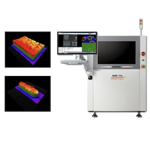
However, all those inspection methods fail to find out hidden solder joint issues such as cavities, cold soldering, and bad tin-soldering adhesion. X-ray inspection system is a type of inspection tool that has been verified to be capable of inspecting hidden solder joints and help establishing and controlling manufacturing process, analyzing prototype and confirming process. Different from MDA, ICT and AOI, an X-ray inspection system is capable of confirming short circuits, open circuits, cavities and BGA solder ball alignment, monitoring process quality and providing instant feedback data for statistical process control (SPC) with high manufacturing efficiency.
X-ray tomography inspection devices can generate tomography images through capturing images of solder joints that are able to implement automatic solder joint analysis and real-time tomography scanning. Moreover, they can carry out accurate comparison analysis on all solder joints of components on both sides of a PCB board within a couple of seconds or two minutes, leading to a conclusion whether solder joints are qualified or not.
BGA Assembly Process and Variation Source
To use X-ray inspection system more effectively, control parameters of BGA assembly process and parameter control limitations have to be clarified. BGA assembly process conforms to the sequence in Figure 1.
When BGA components’ eutectic solder balls are assembled in solder paste during assembly process, their positions are usually corrected through self-alignment of liquid soldering tin. Thus, mounting precision seems not so essential as fine-pitch lead components and the leading control phase in BGA component assembly technology is solder paste printing and reflow soldering. In addition, variation in terms of solder joint shape and size is also associated with many other elements.
It’s almost impossible to eliminate all the variations, so the key point in manufacturing process control is to reduce variation in each manufacturing phase. The influence of different variations on final assembly products should be carefully analyzed and quantitatively processed. With the whole process from BGA components to PCB assembly process considered, leading elements affecting solder joint quality are:
- Volume of solder balls
- BGA component pad size
- PCB pad size
- Solder paste volume
- BGA component deformation during reflow soldering process
- PCB deformation at BGA mounting area during reflow soldering process
- Mounting placement accuracy
- Reflow soldering temperature curve
No matter what type of inspection device is used, there must be a basis when judging whether solder joints are qualified or not. IPC-A-610C regulates the definition of acceptance criteria of BGA solder joints in 12.2.12 item. Excellent BGA solder joints are required to be smooth, round, clear in edge and with no cavities. Diameter, volume, grayscale and contrast should be the same for all solder joints with position aligned and no displacement or twist.
To read the full version of this article, which appeared in the May 2018 issue of SMT007 Magazine, click here.
Share on:


Testimonial
"In a year when every marketing dollar mattered, I chose to keep I-Connect007 in our 2025 plan. Their commitment to high-quality, insightful content aligns with Koh Young’s values and helps readers navigate a changing industry. "
Brent Fischthal - Koh YoungSuggested Items
Absolute EMS: The Science of the Perfect Solder Joint
09/05/2025 | Absolute EMS, Inc.Absolute EMS, Inc., a six-time award-winning provider of fast turnaround, turnkey contract electronic manufacturing services (EMS), is drawing attention to the critical role of 3D Solder Paste Inspection (SPI) in ensuring the reliability of both FLEX and rigid printed circuit board assemblies (PCBAs).
Indium Corporation to Highlight High-Reliability Solder Solutions at SMTA Guadalajara Expo
09/04/2025 | Indium CorporationIndium Corporation, a leading materials refiner, smelter, manufacturer, and supplier to the global electronics, semiconductor, thin-film, and thermal management markets, will feature a range of innovative, high-reliability solder products for printed circuit board assembly (PCBA) at the SMTA Guadalajara Expo and Tech Forum, to be held September 17-18 in Guadalajara, Mexico.
Dr. Jennie Hwang to Present on ‘Solder Joint Reliability’ at SMTA International 2025
09/03/2025 | Dr. Jennie HwangDr. Jennie Hwang to address “Solder Joint Reliability” at the 2025 SMTA International Conference on Monday, October 20. Leveraging her decades of extensive real-world experiences and deep knowledge,
Indium to Highlight Energy-Efficient, High-Reliability Solder Solutions for EV and Electronics at Productronica India
09/03/2025 | Indium CorporationIndium Corporation, a leading materials refiner, smelter, manufacturer, and supplier to the global electronics, semiconductor, electric vehicle (EV), thin-film, and thermal management markets, will feature a range of sustainable, high-reliability solder products at Productronica India, to be held September 17-19 in Bengaluru, India.
Altus Supports Datalink Electronics with Advanced Selective Soldering Solution to Boost Manufacturing Efficiency
09/02/2025 | Altus GroupDatalink Electronics has partnered with Altus Group to integrate a cutting-edge automated soldering solution, enhancing its production capabilities and reinforcing its strategic focus on quality, automation, and scalability.