


 It’s Only Common Sense: The Phone Is Still Mightier Than the Keyboard
 The Marketing Minute: Marketing With Layers


Solution for Next Generation Nanochips Comes Out of Thin Air
November 20, 2018 | RMIT UniversityEstimated reading time: 2 minutes
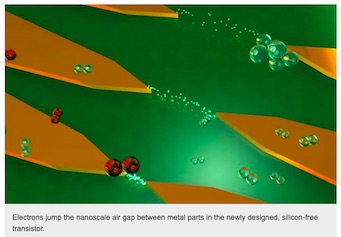
Researchers at RMIT University have engineered a new type of transistor, the building block for all electronics. Instead of sending electrical currents through silicon, these transistors send electrons through narrow air gaps, where they can travel unimpeded as if in space.
The device unveiled in material sciences journal Nano Letters, eliminates the use of any semiconductor at all, making it faster and less prone to heating up.
Lead author and PhD candidate in RMIT’s Functional Materials and Microsystems Research Group, Ms Shruti Nirantar, said this promising proof-of-concept design for nanochips as a combination of metal and air gaps could revolutionise electronics. “Every computer and phone has millions to billions of electronic transistors made from silicon, but this technology is reaching its physical limits where the silicon atoms get in the way of the current flow, limiting speed and causing heat,” Nirantar said.
“Our air channel transistor technology has the current flowing through air, so there are no collisions to slow it down and no resistance in the material to produce heat.”
Moore's Law
The power of computer chips—or number of transistors squeezed onto a silicon chip—has increased on a predictable path for decades, roughly doubling every two years. But this rate of progress, known as Moore’s Law, has slowed in recent years as engineers struggle to make transistor parts, which are already smaller than the tiniest viruses, smaller still.
Nirantar says their research is a promising way forward for nano electronics in response to the limitation of silicon-based electronics. “This technology simply takes a different pathway to the miniaturisation of a transistor in an effort to uphold Moore’s Law for several more decades,” Shruti said.
A New Way Forward
Research team leader Associate Professor Sharath Sriram said the design solved a major flaw in traditional solid channel transistors—they are packed with atoms—which meant electrons passing through them collided, slowed down and wasted energy as heat.
“Imagine walking on a densely crowded street in an effort to get from point A to B. The crowd slows your progress and drains your energy,” Sriram said. “Travelling in a vacuum on the other hand is like an empty highway where you can drive faster with higher energy efficiency.”
But while this concept is obvious, vacuum packaging solutions around transistors to make them faster would also make them much bigger, so are not viable.
“We address this by creating a nanoscale gap between two metal points. The gap is only a few tens of nanometers, or 50,000 times smaller than the width of a human hair, but it’s enough to fool electrons into thinking that they are travelling through a vacuum and re-create a virtual outer-space for electrons within the nanoscale air gap,” he said.
The nanoscale device is designed to be compatible with modern industry fabrication and development processes. It also has applications in space—both as electronics resistant to radiation and to use electron emission for steering and positioning ‘nano-satellites.’
“This is a step towards an exciting technology which aims to create something out of nothing to significantly increase speed of electronics and maintain pace of rapid technological progress,” Sriram said.
This work was undertaken at RMIT University’s cutting-edge Micro Nano Research Facility and with support of the Victorian node of the Australian National Fabrication Facility.
Story: Michael Quin
Share on:


Testimonial
"Advertising in PCB007 Magazine has been a great way to showcase our bare board testers to the right audience. The I-Connect007 team makes the process smooth and professional. We’re proud to be featured in such a trusted publication."
Klaus Koziol - atgSuggested Items
Global Electronics Association Releases Fall Schedule of Instructor-led Courses
10/20/2025 | Corey Lynn, Global Electronics AssociationWhether you’re looking to enhance your PCB design skills, explore advanced packaging technologies, or deepen your understanding of reliability, these Global Electronics Association courses deliver high-impact learning from the best in the industry. Here are a few starting this week.
NOVOSENSE, UAES and Innoscience Advance Power Electronics for New Energy Vehicles
10/20/2025 | PRNewswireThe partnership focuses on developing next-generation intelligent integrated Gallium Nitride (GaN) products. Leveraging their combined expertise, the new devices will deliver more reliable GaN driving and protection features, enabling higher power density and paving the way for wider adoption in automotive systems.
Fabrinet Announces Retirement of Founder and Chairman Tom Mitchell After 25 Years of Visionary Leadership
10/20/2025 | FabrinetFabrinet, a leading provider of advanced optical packaging and precision optical, electro-mechanical and electronic manufacturing services to original equipment manufacturers of complex products, announced the retirement of company founder and Chairman, David T. (Tom) Mitchell, after 25 years of visionary leadership.
PCBA Market Poised to Reach $147.5 Billion by 2035
10/20/2025 | Globe NewswireGlobal printed circuit board assembly market is projected to reach $147.5 billion by 2035, at a CAGR of 4.7% during the forecast period 2025-2035
Marcy’s Musings: The Legislative Outlook—Helping or Hurting?
10/20/2025 | Marcy LaRont -- Column: Marcy's MusingsJust before we were ready to publish our October issue of PCB007 Magazine, some breaking news from the White House, unfortunately (but perfectly) parlayed into why the topic of this month’s issue has been so important to cover in great depth.