


 Trouble in Your Tank: Understanding Interconnect Defects, Part 1
 It’s Only Common Sense: Marketing Isn’t Fluff, It’s Ammunition
 Driving Innovation: Mechanical and Optical Processes During Rigid-flex Production


Graphene Makes Low-Dimensional Spintronics Viable at Room Temperature
January 14, 2019 | CORDISEstimated reading time: 3 minutes
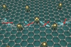
Graphene Flagship researchers produced graphene-based spintronics devices that utilise both electron charge and spin at room temperature. Demonstrating the spin’s feasibility for bridging distances of up to several micrometres, results open up new possibilities for integrating information-processing and storage in a single chip.
From its very inception, the Graphene Flagship programme saw the potential of spintronics devices made from GRMs. Researchers from different universities successfully showed that it is possible to manipulate graphene’s spin properties in a controlled manner at room temperature. These results inspire new directions in the development of spin-logic devices and quantum computing. “With miniaturisation a major driving force behind the electronics industry, graphene opens new possibilities for compacting spin-logic operations with magnetic memory elements in a single platform,” notes Catalan Institution for Research and Advanced Studies (ICREA) Research Professor Stephan Roche, who has been leading the Graphene Flagships Spintronics Work Package since its inception.
Material Imperfections are Not to Blame Any More
Graphene extends the area of spintronics inter-device communication from nanometres to micrometres at low energy cost. Although initial theoretical predictions estimated spin lifetimes of around a microsecond in the material, previous experiments have shown a few nanoseconds at best. This puzzling discrepancy initially suggested that the material’s impurities and defects are primarily responsible for spin relaxation. However, Flagship researchers have challenged these conventionally conceived mechanisms of spin relaxation, and proposed several new ones that are unique to graphene.
In particular, they observed that the rate at which spins relax in systems composed of graphene and transition metal dichalcogenides (TMDCs) strongly depends on whether they are pointing in or out of the graphene plane. “Graphene interfaced with a TMDC could serve as a spin filter, since the transfer of spin information depends on the initial spin polarisation of the injected electrons, enabling new low-power spin-transistor concepts,” explains Prof. Roche.
Importantly, experiments were carried out at room temperature and are particularly important for externally manipulating electron spins in graphene.
The Ultimate Switch
Given that graphene can maintain spin coherence over sufficiently long distances, integrating it with another layered material in which spin is maintained for considerably lesser time can result in fabrication of a spin field-effect transistor-like device. Combining graphene with molybdenum disulfide (MoS2) (where spin lasts for picoseconds), Flagship researchers demonstrated that it is possible to control where the spin can go by using a gate voltage. “This combination of graphene with another thin 2D material with contrasting spintronic properties enables the creation of a spin switch,” observes Prof. Roche.
Researchers have chosen MoS2 due to its low-spin lifetime stemming from its strong spin-orbit coupling. Importantly, this material mix worked at room temperature.
Increasing Spin Signals
From studies of the literature, conductance mismatch has been identified as a key factor that could substantially reduce spin injection from ferromagnets into semiconductors.
The Flagship team showed that they could greatly improve the efficiency of the injection and detection of spin electrons into graphene, by using a sandwich of materials. This consisted of a boron nitride insulator in-between the graphene layer and the ferromagnetic spin injector/detector electrodes.
In the device produced, polarisation increased up to 70 % with voltage, challenging textbook wisdom that only ferromagnets can influence spin polarisation. Instead, quantum tunnelling was found to affect spin polarisation in the devices. In particular, spin bridged a distance of 10 micrometres in more than 3 nanoseconds at room temperature.
“The use of graphene and other 2D materials for advancing next-generation spin torque-based memories (such as STT-MRAM and SOT-MRAM) is also extremely appealing, and has stimulated imec to take the lead of the consortium and work on their large-scale integration in the fab environment,” says Kevin Garello, WP leader and imec researcher leading the emerging magnetic advanced memory concepts research.
Share on:


Testimonial
"Your magazines are a great platform for people to exchange knowledge. Thank you for the work that you do."
Simon Khesin - Schmoll MaschinenSuggested Items
SEMI Foundation Honors Applied Materials at SEMICON West with 2025 Excellence in Achievement Award for Talent Development
11/04/2025 | SEMIThe SEMI Foundation announced it recognized Applied Materials, Inc. with the Excellence in Achievement Award at SEMICON West 2025 in Phoenix, Arizona, honoring the company’s outstanding leadership and collaboration in building the next generation of semiconductor talent.
Sealed for Survival: Potting Electronics for the Toughest Environments
10/29/2025 | Beth Massey, MacDermid Alpha Electronics SolutionsElectronics deployed in harsh conditions face relentless threats from vibration, impact, chemical contaminants, airborne pollutants, and moisture, conditions that can quickly lead to failure without robust protection. Potting, the process of encapsulating electronics in a protective polymer, is a widely used strategy to safeguard devices from both environmental and mechanical hazards.
Driving Innovation: Mechanical and Optical Processes During Rigid-flex Production
10/28/2025 | Kurt Palmer -- Column: Driving InnovationRigid-flex printed circuit boards are a highly effective solution for placing complex circuitry in tight, three-dimensional spaces. They are now indispensable across a range of industries, from medical devices and aerospace to advanced consumer electronics, helping designers make the most efficient use of available space. However, their unique construction—combining rigid and flexible materials—presents a fundamental challenge for PCB manufacturers.
SMTAI 2025 Review: Reflecting on a Pragmatic and Forward-looking Industry
10/27/2025 | Marcy LaRont, I-Connect007Leaving the show floor on the final afternoon of SMTA International last week in Rosemont, Illinois, it was clear that the show remains a grounded, technically driven event that delivers a solid program, good networking, and an easy space to commune with industry colleagues and meet with customers.
ITW EAE Despatch Ovens Now Support ASTM 5423 Testing
10/15/2025 | ITW EAEAs the demand for high-performance electrical insulation materials continues to grow—driven by the rapid expansion of electric vehicles (EVs) and energy storage systems—thermal processing has become a critical step in material development.