-

-
News
News Highlights
- Books
Featured Books
- smt007 Magazine
Latest Issues
Current Issue
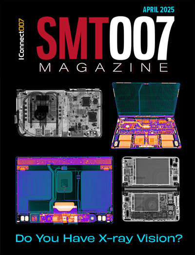
Do You Have X-ray Vision?
Has X-ray’s time finally come in electronics manufacturing? Join us in this issue of SMT007 Magazine, where we answer this question and others to bring more efficiency to your bottom line.

IPC APEX EXPO 2025: A Preview
It’s that time again. If you’re going to Anaheim for IPC APEX EXPO 2025, we’ll see you there. In the meantime, consider this issue of SMT007 Magazine to be your golden ticket to planning the show.

Technical Resources
Key industry organizations–all with knowledge sharing as a part of their mission–share their technical repositories in this issue of SMT007 Magazine. Where can you find information critical to your work? Odds are, right here.
- Articles
- Columns
Search Console
- Links
- Media kit
||| MENU - smt007 Magazine
ICT or Flying Probe: Which Test Is Best for Your Assembly?
July 10, 2019 | Russell Poppe, JJS ManufacturingEstimated reading time: 3 minutes
In-circuit test (ICT) and flying probe are two of the most popular types of automated test equipment (ATE) used in electronic printed circuit board assembly (PCBA). But what sets them apart? And how can you decide on the test strategy that is going to work best for your assemblies? In this article, I highlight the benefits (and the shortcomings) of both ICT and flying probe with a specific focus on three areas: product design, coverage, and cost.
1. Product Design
A good quality test program (also known as good coverage) will rely on the quality of your computer-aided design (CAD) data and schematics. The CAD data is used to generate the basic test programme, which ensures that information is sourced from the original design rather than any manual interpretation of other data. Good quality populated, and unpopulated, sample PCBAs are also vital for fine-tuning the test programmes, debugging, and making any fixtures so that the assemblies physically fit as they were intended.
Thinking about product design for a moment, what are the differences between each test solution which you may want to keep in mind? Flying probe machines, like those offered by Takaya, can probe the ends of component pads and uncovered vias to get access to the electrical networks. ICT will require at least a 50thou wide test pad per net, which has been designed into the PCB upfront and is used as a target for the fixed test probe. Double-sided fixtures can be costly, so these should, ideally, be on one side only of the PCB.
2. Coverage
When I talk about coverage, I’m referring to how much of the circuit you are actually able to test. Both ICT and flying probe carry out what is called a manufacturing defects analysis (MDA), which allows for the majority of the most common process faults that are likely to occur. These can include open circuits (due to insufficient or faulty soldering), short circuits, passive component measurements (resistors and capacitors), diode and transistor orientation, and basic supply voltage measurements.
However, given that these elements are common to both types of the testing platform, what sets them apart?
- Most flying probe systems will offer some form of limited optical inspection, which adds coverage for those components that can’t be accessed electrically; ICT fixtures usually won’t offer the option of optical inspection
- In addition to vectorless test, integrated circuits (ICs) can also include some powered (albeit basic) functional testing to check the soldering of pins to the PCB through a non-contact capacitive probe or plate; in most cases, flying probe is limited to only vectorless test
- ICT can also provide limited analogue and digital measurements, which flying probe isn't capable of due to the limited number of probes
3. Cost
The programming cost will depend on the complexity of the assembly but is broadly the same for either test solution (potentially around $2,500 or so). When it comes to other charges associated with test, however, there are some key differences to bear in mind:
- The fixture costs of flying probe are usually zero; in contrast, an ICT fixture can run to nearly $5,000
- The development lead time for flying probe is typically less than a week; ICT can take up to six weeks for fixture manufacture and programming
- In the event that your product design changes in any way, it will only require a programme change; in the case of ICT, it could well require a new fixture as well if any components or test pads have moved
- The actual machine test time of ICT is usually less than a minute, which means it is ideal for working quickly through larger batches; flying probe, on the other hand, can take several minutes, which means it's often more suited to smaller batches
- The speed of ICT also means that it is relatively inexpensive, often coming in at less than $1.24 per unit; flying probe is a much slower process and can cost $62 or more per assembly)
If you're still unsure about which test option is best for your product, you may find this simple visual checklist useful in comparing the pros and cons:
When it comes to test, each product will have its own unique requirements. But by keeping in mind the primary benefits (and points of difference) of the two platforms, you should feel much better placed to select the best test strategy for your PCBA assembly.
Russell Poppe is the director of technology at JJS Manufacturing.
Suggested Items
CCL Design, Ynvisible Announce Strategic Partnership to Deliver Scalable Printed Display Solutions
04/28/2025 | CCL DesignCCL Design will integrate Ynvisible's proprietary display technology into its global manufacturing infrastructure and technology portfolio.
Siemens, TSMC Extend Collaboration to Drive Semiconductor Design Innovation
04/25/2025 | SiemensSiemens Digital Industries Software announced that the company has deepened longstanding collaboration with TSMC to drive innovation in semiconductor design and integration, enabling mutual customers to tackle the challenges of next-generation technologies.
Ansys Strengthens Collaboration with TSMC on Advanced Node Processes Certification and 3D-IC Multiphysics Design Solutions
04/24/2025 | PRNewswireThrough continued collaboration with TSMC, Ansys announced enhanced AI-assisted workflows for radio frequency (RF) design migration and photonic integrated circuits (PICs), and new certifications for its semiconductor solutions. Together,
Autodesk Donates $4.3 Million to Cornell University to Prepare students for an AI-powered future
04/24/2025 |Autodesk announced a $4.3 million gift to Cornell University’s College of Engineering and College of Architecture, Art, and Planning (AAP) to help prepare students for the future of work in an increasingly AI-driven world. The investment will fund a new Autodesk Cornell Engineering Design and Make Space in Upson Hall.
Driving Sustainability in PCB Design
04/24/2025 | Marcy LaRont, I-Connect007Filbert (Fil) Arzola is an electrical engineer at Raytheon. He’s smart, entertaining, and passionate about PCB design. As it turns out, he’s also passionate about “Mother Earth,” as he calls her. Born and raised in Southern California, he freely admits that he turns the water off when he brushes his teeth and yells at his brother for throwing batteries in the garbage. But when looking at the issue of sustainability and PCB design, he urges his audiences to ponder what sustainability looks like. Can PCB designers, he asks, make any impact on sustainability at all?


