


 Trouble in Your Tank: Understanding Interconnect Defects, Part 1
 It’s Only Common Sense: Marketing Isn’t Fluff, It’s Ammunition
 Driving Innovation: Mechanical and Optical Processes During Rigid-flex Production


Researchers Realize World’s Thinnest Optical Hologram with 2-D Material Monolayer
August 22, 2019 | Missouri S&TEstimated reading time: 2 minutes
Missouri S&T researchers are demonstrating a new concept to reconstruct holographic images by using a single two-dimensional material monolayer with the thickness of less than one nanometer. Their work could lead to the creation of smart watches with holographic displays, printed security cryptograms on bank notes and credit cards, and new possibilities for data storage.
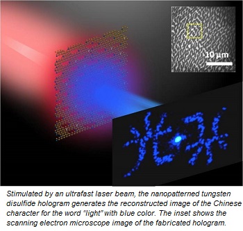
The researchers describe their atomically thin nonlinear optical holograms in Nano Letters, one of the top journals in nanotechnology research, and prototype their device by reconstructing several kinds of holographic images with tungsten disulfide monolayers of the thickness of around 0.7 nanometer. A nanometer is one billionth of a meter, and a tungsten disulfide monolayer only contains one layer of tungsten atoms sandwiched between two layers of sulfur atoms.
The approach is described in the Nano Letters paper “Atomically thin nonlinear transition metal dichalcogenide holograms,” which was published online Friday, Aug. 16. It involves the use of only a single nanopatterned tungsten disulfide monolayer that is able to control the wavefront of light, where the designed hologram patterns are punctured by a nanofabrication process known as focused ion beam milling.
Experimenting with the ultrafast laser excitation on the nanopatterned tungsten disulfide monolayer, the researchers demonstrated a nonlinear optical hologram with high conversion efficiency and atomic thickness, for producing optical vortex beams and Airy beams as well as reconstructing complex holographic images at the second harmonic frequency. An Airy beam is a waveform that appears to curve as it moves.
In their paper, the Missouri S&T researchers published reconstructed holographic images of the Chinese character for the word “light” with blue and green colors. They believe this new type of optical hologram holds promise for future applications, such as security markings on banknotes and credit cards, optical communications, smart watch displays, and data storage.
“We are able to control the binary amplitude modulation of zero and one by simply etching out or keeping the tungsten disulfide monolayer area,” says Dr. Xiaodong Yang, an associate professor in mechanical and aerospace engineering at Missouri S&T. “Our holograms possess significantly higher nonlinear conversion efficiency than the currently existing plasmonic metasurface holograms made of metallic nanostructures.”
“In addition, our holograms have atomic thickness of less than one nanometer, much thinner than the usual thickness of tens of nanometers for plasmonic metasurfaces and several hundred nanometers for dielectric metasurfaces,” says Dr. Jie Gao, an associate professor of mechanical and aerospace engineering at Missouri S&T and co-author of the paper.
Share on:


Testimonial
"In a year when every marketing dollar mattered, I chose to keep I-Connect007 in our 2025 plan. Their commitment to high-quality, insightful content aligns with Koh Young’s values and helps readers navigate a changing industry. "
Brent Fischthal - Koh YoungSuggested Items
Nortech Systems Incorporated Earns AS9100 Certification for Monterrey, Mexico Facility
11/04/2025 | BUSINESS WIRENortech Systems, Incorporated, a leading provider of design and manufacturing solutions for complex electromedical devices and electromechanical systems, announced that its Monterrey, Mexico, facility has achieved AS9100:D certification.
PsiQuantum, Lockheed Martin Form Strategic Collaboration to Accelerate Quantum Computing for Aerospace and Defense
11/04/2025 | BUSINESS WIREPsiQuantum and Lockheed Martin have signed a memorandum of understanding (MoU) to accelerate the development of quantum computing applications in aerospace and defense.
Aircraft Wire and Cable Market to surpass USD 3.2 Billion by 2034
10/30/2025 | Global Market Insights Inc.The global aircraft wire and cable market was valued at USD 1.8 billion in 2024 and is estimated to grow at a CAGR of 5.9% to reach USD 3.2 billion by 2034, according to recent report by Global Market Insights Inc.
Honeywell Announces Updated Business Segment Structure Ahead Of Aerospace Spin-Off
10/28/2025 | HoneywellHoneywell announced its updated business segment structure ahead of the planned separation of its Aerospace Technologies business, expected in the second half of 2026, and its Solstice Advanced Materials business, expected to be completed on October 30, 2025.
Lockheed Martin Signs Strategic Partnership Framework with Korean Air
10/28/2025 | Lockheed MartinLockheed Martin is collaborating with Korean Air to explore opportunities to support the U.S. government’s (USG) Regional Sustainment Framework (RSF) initiative, as well as expand Maintenance, Repair, Overhaul & Upgrade (MROU) cooperation to third-country markets.