


 Trouble in Your Tank: Implementing Direct Metallization in Advanced Substrate Packaging
 It’s Only Common Sense: Storytelling That Sells—Stop Pitching, Start Painting Pictures
 The Right Approach: Get Ready for ISO 9001 Version 6


An Industrial Collaboration for Thermally Controlled 3D-Printed Metal/Polymer Components
September 3, 2019 | IMDEA NanocienciaEstimated reading time: 1 minute
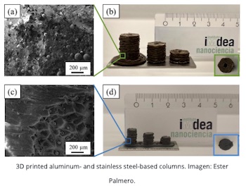
IMDEA Nanociencia’s research led by Dr. Palmero jointly with the company RAMEM has resulted in successful development of thermally controlled 3D-printed proof-of-concept metallic/polymer components. This work constitutes an industrial collaboration with applicability in the aeronautic and aerospace sectors.
One of the main technological challenges when trying to combine metal particles with polymers for the fabrication of functional composites is the possibility of achieving a high metal concentration dispersed in a suitable polymer. Not every polymer is valid for the synthesis of metal-based composites since issues such as solubility are crucial. Challenges extend after the synthesis of the composite to the fabrication of a continuous wire or filament to achieve a high metal content and not just a polymeric product with dispersed metallic particles. This is of extreme importance to end with 3D-printed metal/polymer components providing high thermal conductivity (when needed) and mechanical stability in view of practical applications.
The technological novelty of the work developed by IMDEA Nanociencia and RAMEM comprises: 1) identification of polymers (acrylonitrile butadiene styrene, ABS) adequate to be combined with metallic particles (aluminum and stainless steel) for the synthesis of composites through a scalable method; 2) fabrication of continuous filaments (above 15 m long as proof-of-concept) with high flexibility and a high metal content of 80%; and 3) thermally controlled printing of components using metal/polymer filament, with no need of going to laser assisted methods. This 3D-printing method allows a personalized manufacturing and creation of complex and light geometries.
The fabrication method proposed by Dr. Palmero and coworkers eliminates manufacturing and postprocessing equipment and tooling, and minimizes material waste, saving in this way significant manufacturing cost. Moreover, this thermally controlled 3D-printing method might be combined with standard additive manufacturing technologies for the fabrication of multimaterial and multifunctional metallic components.
In view of potential technological applications in sectors such as aeronautics and aerospace, this work could open a new path (from the composite synthesis to the 3D-printing process) for the fabrication of pieces with controlled and tuned amount of metallic particles, arbitrary designs, and in consequence, tuned physical properties.
Share on:


Testimonial
"Our marketing partnership with I-Connect007 is already delivering. Just a day after our press release went live, we received a direct inquiry about our updated products!"
Rachael Temple - AlltematedSuggested Items
Panasonic Industry will Double the Production Capacity of MEGTRON Multi-layer Circuit Board Materials Over the Next Five Years
09/15/2025 | Panasonic Industry Co., Ltd.Panasonic Industry Co., Ltd., a Panasonic Group company, announced plans for a major expansion of its global production capacity for MEGTRON multi-layer circuit board materials today. The company plans to double its production over the next five years to meet growing demand in the AI server and ICT infrastructure markets.
Sustainability and Selective Soldering
09/15/2025 | Dr. Samuel J. McMaster, Pillarhouse InternationalSustainability is more than just a buzzword for the electronics industry; it’s a key goal for all manufacturing processes. This is more than a box-ticking exercise or simply doing a small part for environmentally friendly processes. Moving toward sustainable solutions drives innovation and operational efficiency.
ASM Technologies Limited signs MoU with the Guidance, Government of Tamilnadu to Expand Design-Led Manufacturing capabilities for ESDM
09/15/2025 | ASM TechnologiesASM Technologies Limited, a pioneer in Design- Led Manufacturing in the semiconductor and automotive industries, announced signing of Memorandum of Understanding (MoU) with the Guidance, Government of Tamilnadu whereby it will invest Rs. 250 crores in the state to expand its ESDM related Design-Led Manufacturing and precision engineering capacity. ASM Technologies will acquire 5 acres of land from the Government of Tamilnadu to set up a state-of-the-art design facility in Tamil Nadu's growing technology manufacturing ecosystem, providing a strong strategic advantage and long-term benefits for ASM.
U.S. CHIPS Act Funding Detailed on SIA Website
09/12/2025 | Nolan Johnson, I-Connect007The U.S. CHIPS Act has moved well into the implementation stage in 2025. But where has that money gone? The Semiconductor Industry Association has been tracking these projects and provides details on its website. It was updated May. Among the five key programs being managed under CHIPS, two stand out as influencing advanced electronic packaging: the National Advanced Packaging Manufacturing Program (NAPMP), and the CHIPS Manufacturing USA Institute (MFG USA).
Zhen Ding Drives AI-Powered Digital Transformation
09/12/2025 | Zhen DingDriven by the surging demand for computing power fueled by AI, the semiconductor and PCB industries are forging closer integration, expanding their ecosystems, and pursuing shared growth. PCB has already become another NT$ trillion-dollar industry in Taiwan, growing in tandem with the semiconductor sector.