


 It’s Only Common Sense: Marketing Isn’t Fluff, It’s Ammunition
 Driving Innovation: Mechanical and Optical Processes During Rigid-flex Production
 The Chemical Connection: Onshoring PCB Production—Daunting but Certainly Possible


SCHMID Group Installs PlasmaLine at Hofstetter PCB AG
November 8, 2019 | SCHMID GroupEstimated reading time: Less than a minute
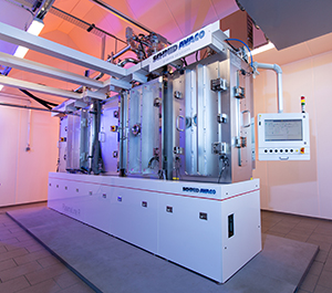
SCHMID Group installed first PlasmaLine comprising ICP etch and sputter deposition of its Korean JV SCHMID AVACO at Hofstetter PCB AG in Switzerland.
It is PlasmaLine D-R tool intended for process development and small scale production (up to 20 half-panels per hours for upgraded tool).
PlasmaLine is a series of modular inline plasma systems for touch-free, simultaneous double-sided or single-sided vertical processing of high end HDI+ PCBs and IC substrates with a capacity of up to 4 panels/min. By combining etch and sputtering process modules, the system can be configured flexibly for almost any application.
These advantages make the PlasmaLine to a new state of the art solution for high frequency applications, mSAP, SAP and embedding boards:
- High flexibility of materials which can be processed
- Increased capabilities of high copper adhesion
- Low roughness
- High energy savings
Curious? Meet us at productronica Munich, Nov. 12.-15.2019, Hall B3, Booth no. 205
Share on:


Testimonial
"The I-Connect007 team is outstanding—kind, responsive, and a true marketing partner. Their design team created fresh, eye-catching ads, and their editorial support polished our content to let our brand shine. Thank you all! "
Sweeney Ng - CEE PCBSuggested Items
Unlocking the Promise of AI in Electronics Manufacturing
10/29/2025 | Shobhit Agrawal, Keysight TechnologiesThe electronics manufacturing industry is rapidly evolving as more complicated products are introduced in the production lines, which require technological advancements even in the production processes. The requirements for production that is efficient, product quality that is greater, and product life cycles that are shorter are more crucial than ever before. In the electronic device life cycle, from design to maintenance, test phases have a significant impact on the economy of the company. Test processes are closely linked to the production volume and impacted by the complexity of the product. For businesses to maintain their competitive edge, they need to adopt innovative solutions and redefine processes.
Connect the Dots: Designing for the Reality of UHDI PCBs—Drilling
11/04/2025 | Matt Stevenson -- Column: Connect the DotsUltra high density interconnect (UHDI) PCBs are changing the game in designing for the reality of manufacturing. With both consumer and industrial electronic devices becoming more advanced, the demand for UHDI PCBs will grow. That means we’re all likely to be designing more UHDI boards. UHDI advanced miniaturization technology challenges designers with regard to both board thickness and footprint. Designers will face more variables in every aspect of design creation. This is certainly the case with drilling.
Driving Innovation: Mechanical and Optical Processes During Rigid-flex Production
10/28/2025 | Kurt Palmer -- Column: Driving InnovationRigid-flex printed circuit boards are a highly effective solution for placing complex circuitry in tight, three-dimensional spaces. They are now indispensable across a range of industries, from medical devices and aerospace to advanced consumer electronics, helping designers make the most efficient use of available space. However, their unique construction—combining rigid and flexible materials—presents a fundamental challenge for PCB manufacturers.
SMTAI 2025 Review: Reflecting on a Pragmatic and Forward-looking Industry
10/27/2025 | Marcy LaRont, I-Connect007Leaving the show floor on the final afternoon of SMTA International last week in Rosemont, Illinois, it was clear that the show remains a grounded, technically driven event that delivers a solid program, good networking, and an easy space to commune with industry colleagues and meet with customers.
The Marketing Minute: Marketing With Layers
10/15/2025 | Brittany Martin -- Column: The Marketing MinuteMarketing to a technical audience is like crafting a multilayer board: Each layer serves a purpose, from the surface story to the buried detail that keeps everything connected. At I-Connect007, we’ve learned that the best marketing campaigns aren’t built linearly; they’re layered. A campaign might start with a highly technical resource, such as an in-depth article, a white paper, or a podcast featuring an engineer delving into the details of a process. That’s the foundation, the substance that earns credibility.