


 Global PCB Connections: Rigid-flex and Flexible PCBs—The Backbone of Modern Electronics
 Flexible Thinking: The Key to a Successful Flex Circuit Design Transfer
 Happy’s Tech Talk #29: Bend-to-Install Semi-flex FR-4


HARTING’s Component Carrier Can Replace Flexible PCBs
July 15, 2020 | PR NewswireEstimated reading time: 4 minutes
Flexible printed circuit boards made of thin polyimide films have established themselves in many product areas thanks to their application flexibility. Populating and assembling them, however, is decidedly more complex. This is where a newly developed component carrier from HARTING enters the picture.
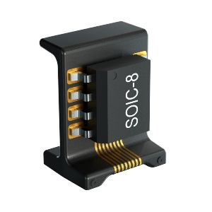
A standardised component carrier for electronic components
By harnessing this all new HARTING development, electronic components can be fitted directly onto the component carrier, thereby replacing flexible circuit boards. The component carrier serves as a connecting element between the printed circuit board (PCB) and electronic components such as LEDs, ICs, photodiodes and sensors.
The populated component carriers are delivered in tape & reel. In their standard design, the carriers can be processed in automatic assembly systems, just like other SMD electronic components. Two different sizes are currently available and can accommodate electronic components of standard size SOIC-8 and smaller. Moreover, HARTING can also produce the carriers in customer-specific sizes.
HARTING has identified three example applications where the component carrier can replace flexible circuit boards:
- Components at a 90° angle to the circuit board: The component carrier is suitable for scenarios in which electrical components, such as sensors, need to be positioned normal to the circuit board. The automatic assembly process enables the placement of temperature sensors or hall sensors on the carrier to a high degree of accuracy, which in turn results in precise, reproducible measurements. Optical components are another salient example, such as LEDs or photodiodes used to generate precise light barriers.
- Clearance from the circuit board: The component carrier also makes it possible to maintain a clearance between the circuit board and an electronic component. Consequently, a temperature sensor can be used to measure the temperature in the housing without being influenced by the waste heat from other components on the PCB. It also means that an LED can be placed clear of the circuit board, thereby avoiding the risk of surrounding components casting shadows.
- Antenna function: The component carrier can be manufactured using different base polymers. In this way, different antenna material properties can be factored in, such as dielectric constant and loss factor. The specific antenna layout can be used for various applications in the MHz and GHz frequency range, such as Bluetooth, WiFi, ZigBee and 5G.
3D-MID technology as an alternative to flexible PCBs
Thanks to the 3D-MID (mechatronic integrated device) technology, electronic components can be fitted directly onto a three-dimensional body without the need for circuit boards or connecting cables. The base body is produced through injection moulding, whereby the thermoplastic is provided with a non-conductive, inorganic additive. In order for this material to be able to accommodate electrical circuits, the additives in the plastic are "activated" through laser direct structuring (LDS). In this process, the laser beam writes the areas intended for the conductive tracks and creates a micro-rough structure. The metal particles released in the process form the nuclei for the subsequent chemical metallisation.
This process creates electrical traces across the three-dimensional base body. The plastic employed offers high thermal stability and can therefore be soldered in the reflow oven.
HARTING has been implementing the entire 3D-MID process chain in-house for over 10 years, from the project idea to the populated series product. The technology is finding use in application scenarios in areas such as medical technology, industrial electronics and consumer electronics and all the way through to safety-related components in the automotive industry. The HARTING 3D-MID business unit is the largest provider of 3D-MID components outside of Asia.
The component carrier developed by this process is suitable for various applications. It can be equipped with several sensors that, if desired, could be aligned in three directions to take measurements in three axes (X, Y, Z). Components can be fitted simultaneously on two parallel surfaces on the front and back sides, as well as on the end face. HARTING has submitted a patent application for the component carrier.
The component carrier cuts costs by two-thirds
In an automated process, HARTING fits electronic components such as LEDs, ICs, photodiodes and sensors directly on the component carrier. The total cost of the component carrier is two-thirds lower than those of flexible PCB solutions. This is due to the fact that it eliminates the frequently complex handling involved with flexible printed circuit boards, e.g. populating, gluing and assembling. The process even delivers benefits in small volumes, as the component carrier can be used for different applications without adaptation, thereby eliminating the costs of a new injection mould. Compared with flexible printed circuit boards, this process achieves more precise component positioning, greater repeatability and better quality.
HARTING has identified another advantage of the component carrier, namely the short timeframe required to deliver finished components. Since the plastic carrier remains unchanged, all that is needed are specifications for placement of the electronic components. Experts in 3D-MID can use this to create a production-optimised layout proposal. Adjustments of the laser program are all that is needed to tailor the electrical traces to the respective application. Once the customer has approved the product and components have been received, initial production samples can be dispatched within two to three weeks – and even faster, if necessary.
Share on:


Testimonial
"Our marketing partnership with I-Connect007 is already delivering. Just a day after our press release went live, we received a direct inquiry about our updated products!"
Rachael Temple - AlltematedSuggested Items
The Marketing Minute: Marketing With Layers
10/15/2025 | Brittany Martin -- Column: The Marketing MinuteMarketing to a technical audience is like crafting a multilayer board: Each layer serves a purpose, from the surface story to the buried detail that keeps everything connected. At I-Connect007, we’ve learned that the best marketing campaigns aren’t built linearly; they’re layered. A campaign might start with a highly technical resource, such as an in-depth article, a white paper, or a podcast featuring an engineer delving into the details of a process. That’s the foundation, the substance that earns credibility.
Taking Control of PCB Verification One Step at a Time
10/09/2025 | Kirk Fabbri, Siemens EDAToday’s designs are as complex as ever, and engineers face tough decisions every day. Simulation and verification teams are confronted with a three-fold challenge: understanding the underlying theory, mastering the tools, and applying best practices.Engineers need to navigate a vast and ever-changing cast of design and simulation tools, often with overlapping functionality.
Happy’s Tech Talk #43: Engineering Statistics Training With Free Software
10/06/2025 | Happy Holden -- Column: Happy’s Tech TalkIn over 50 years as a PCB process engineer, the one skill I acquired in college that has been most beneficial is engineering statistics. Basic statistics was part of my engineering fundamentals classes, but I petitioned the dean to let me take the engineering statistics graduate course because I was creating a senior thesis for my honors focus and needed more training on Design of Experiments (DOE).
Connect the Dots: Evolution of PCB Manufacturing—Lamination
10/02/2025 | Matt Stevenson -- Column: Connect the DotsWhen I wrote The Printed Circuit Designer's Guide to...™ Designing for Reality, it was not a one-and-done effort. Technology is advancing rapidly. Designing for the reality of PCB manufacturing will continue to evolve. That’s why I encourage designers to stay on top of the tools and processes used during production, to ensure their designs capitalize on the capabilities of their manufacturing partner.
Empower Sets New Benchmark with 20x Faster Response and Breakthrough Sustainability Demonstrated at OCP Global Summit 2025
09/25/2025 | Empower SemiconductorEmpower Semiconductor, the world leader in powering AI-class processors, announced that its Crescendo chipset, an artificial intelligence (AI) and high-performance computing (HPC) processor true vertical power delivery platform, is available now for final sampling, with mass production slated for late 2025.