


 Dan’s Biz Bookshelf: ‘In Defense of a Liberal Education’
 American Made Advocacy: A Growing Presence in Washington in Turbulent Times
 It’s Only Common Sense: How to Win Back Lost Customers


Aurora Circuits on Ultra-Heavy Copper PCBs
August 3, 2020 | Dan Beaulieu, D.B. Management GroupEstimated reading time: 3 minutes
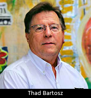
It’s always fun to talk with a company that can do something different—in this case, ultra-heavy copper PCBs, meaning over 20-ounce copper. Wanting to know more about this, I talked to Aurora Circuits Director of Business Development Thad Bartosz, who is one of our industry experts when it comes to ultra-heavy copper technology.
Dan Beaulieu: Thad, it’s good talking to you today. Let’s start with the basics. What is heavy copper?
Thad Bartosz: Heavy copper used to be defined as 4–5 ounce, but we do that for a snack. Aurora is capable of fabricating SS, NPTH, PTH, and multilayer types with up to 20-oz copper layers.
Beaulieu: What defines ultra-heavy copper?
Bartosz: Ounces of copper have been defined in ounces per square foot of area on the process panel. The thickness of the copper foil is based on 0.0014” per oz. Copper weights of 4–5 ounces are made with electrodeposited copper (ED), and ultra-heavy copper sheets are made with rolled annealed (RA) copper that must be treated to laminate to dielectrics used in fabrication.
Beaulieu: How many ounces of copper can you do at Aurora?
Bartosz: We have delivered PCBs with etched copper up to 20 ounces and would work with customers that may require any copper thickness.
Beaulieu: Why doesn’t every shop build this technology?
Bartosz: You need to have the proper equipment and process capabilities—some of these are customer or Aurora proprietary—so that you can fabricate a usable product that meets customer requirements.
Beaulieu: How did you get involved with this technology?
Bartosz: We have been building ultra-heavy copper products since 2003 when a customer asked if we could do this as they were having issues with their current source.
Beaulieu: What special equipment and processes do you have that allow you to build ultra-heavy copper boards?
Bartosz: As I mentioned earlier, these are processes that have been developed over years of sampling and production processing. We start with a sample run to establish a feasible process and then scale up for production. Etching is normally a big factor as well as machining, so you acquire equipment to properly process the PCB to make an acceptable finished product.
Beaulieu: What technology requires ultra-heavy copper?
Bartosz: Circuit boards that need high current or thermal dissipation like solar and wind power collection, aerospace/military, telecommunications, and automotive applications.
Beaulieu: What kind of end-products need it?
Bartosz: Some products include automotive junction boxes, battery management systems, and high-power circuits that have MOSFETs, IGBTs, and other high-current components, running hundreds of amps through the circuitry. For those who may not know, MOSFETs and IGBTs are a couple of power devices/components that can handle high-voltage and high-current needs. You will find them on inverters, converters, and power supplies.
Beaulieu: How do you think it will be used in the future?
Bartosz: Currently, designs have been made for power distribution, power collection, battery-powered transportation, and LED lighting. Future use will depend on new applications needed in the marketplace. You also need a supplier that changes with the market to meet these specialized needs. It will definitely be used more in the future.
Beaulieu: Is this kind of technology being designed right now?
Bartosz: Yes, it is still used in the automotive and power markets, such as new EV and autonomous vehicles where battery technology has higher current requirements and power-generation systems, solar, wind, or conventional types as their technology changes.
Beaulieu: How many ultra-heavy copper boards have you built?
Bartosz: Aurora has shipped over five million boards of single-sided, PTH, and multilayer designs over the last 10 years. Many of these were for junction boxes or battery systems in automobiles. For a few years, we shipped over 400,000 6/6 copper PCBs to China. We have processed over 800 tons (based on oz/sq ft) and over 1.7 million square feet without any EPA violations.
Beaulieu: Before we end, tell us a little bit about Aurora Circuits.
Bartosz: We have over 60 years of experience in printed circuit fabrication, providing advanced thermal management and interconnect technology solutions for PCB designs and specialty products. Product specialty areas include polymer thick-film (PTF) resistors, metal-clad materials for LED lighting and other markets, durable plating for contact areas, and, of course, ultra-heavy copper. We partner with companies to help them to maximize profitability and production sustainability.
Beaulieu: Thank you, Thad.
Bartosz: No problem, Dan.
Read more about Aurora Circuits and ultra-heavy copper PCBs here.
Share on:


Testimonial
"Advertising in PCB007 Magazine has been a great way to showcase our bare board testers to the right audience. The I-Connect007 team makes the process smooth and professional. We’re proud to be featured in such a trusted publication."
Klaus Koziol - atgSuggested Items
Statement from the Global Electronics Association on the July 2025 Tariff on Copper Foil and Electronics-Grade Copper Inputs
07/31/2025 | Global Electronics AssociationWe are disappointed by today’s decision to impose a 50% tariff on imported copper foil and other essential materials critical to electronics manufacturing in the United States.
Considering the Future of Impending Copper Tariffs
07/30/2025 | I-Connect007 Editorial TeamThe Global Electronics Association is alerting industry members that a potential 50% tariff on copper could hit U.S. electronics manufacturers where it hurts.
Connect the Dots: Sequential Lamination in HDI PCB Manufacturing
07/31/2025 | Matt Stevenson -- Column: Connect the DotsAs HDI technology becomes mainstream in high-speed and miniaturized electronics, understanding the PCB manufacturing process can help PCB design engineers create successful, cost-effective designs using advanced technologies. Designs that incorporate blind and buried vias, boards with space constraints, sensitive signal integrity requirements, or internal heat dissipation concerns are often candidates for HDI technology and usually require sequential lamination to satisfy the requirements.
OKI Launches Rigid-Flex PCBs with Embedded Copper Coins Featuring Improved Heat Dissipation for Space Equipment Applications
07/29/2025 | BUSINESS WIREOKI Circuit Technology, the OKI Group’s printed circuit board (PCB) business company, has developed rigid-flex PCBs with embedded copper coins that offer improved heat dissipation for use in rockets and satellite-mounted equipment operating in vacuum environments.
Designers Notebook: Basic PCB Planning Criteria—Establishing Design Constraints
07/22/2025 | Vern Solberg -- Column: Designer's NotebookPrinted circuit board development flows more smoothly when all critical issues are predefined and understood from the start. As a basic planning strategy, the designer must first consider the product performance criteria, then determine the specific industry standards or specifications that the product must meet. Planning also includes a review of all significant issues that may affect the product’s manufacture, performance, reliability, overall quality, and safety.