


 Global PCB Connections: Rigid-flex and Flexible PCBs—The Backbone of Modern Electronics
 Flexible Thinking: The Key to a Successful Flex Circuit Design Transfer
 Happy’s Tech Talk #29: Bend-to-Install Semi-flex FR-4


PV Nano Cell, Profactor Publish Results of Printed Embedded Passive Components
October 20, 2020 | Globe NewswireEstimated reading time: 2 minutes
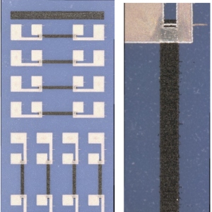
PV Nano Cell, Ltd., an innovative provider of inkjet-based conductive digital printing solutions and producer of conductive digital inks and PROFACTOR GmbH (Steyr, Austria) an applied production research company in the field of industrial assistive systems and additive micro/nano manufacturing, published the first results of printed embedded passive components including silver and carbon-based resistors and capacitors. PV Nano Cell, Profactor and other partners are part of the EU inkjetPCB project (E! 113206, supported by the prestigious eurostars™ program in the Horion2020 framework) which is focused on the fabrication of multilayer printed circuit boards with embedded printed passive components.
As previously published, the use of electronic devices is increasing and so does the demand for high performing, smaller-sized products. One way to enable such products is by implementing embedded passive components such as resistors and capacitors. Instead of placing these components on the PCB (Printed Circuit Board), the components can be embedded within the PCB layers. Such an approach clears valuable real estate on the top or bottom side of the PCB allowing for more powerful CPUs or batteries to be incorporated in the electronic device. Existing PCB manufacturing technologies are complex and involve many production stages. Furthermore, such subtractive technologies where production material is removed during the production are very costly due to the high use of material and production waste. Digital printing however, is an additive technology where material is added only where required and therefore solves these problems and offers new advantages.
PV Nano Cell’s Chief Executive Officer, Dr. Fernando de la Vega, commented, “PV Nano Cell is aiming to commercialize digital printing of embedded passive components very soon, using a technology based on our DemonJet printers and Sicrys™ inks. We will enable the industry to print embedded conductive traces, resistors, capacitors and coils allowing new electronic designs. Some of the development efforts are within the scope of InkjetPCB project. InkjetPCB is a European consortium funded by eurostars™ framework, technical-led by our partner Profactor, a world leader applied research institute focusing in additive manufacturing of electronics. The project is focusing on Inkjet-based fabrication of multilayer printed circuit boards with embedded printed passive elements as a commercially viable process. As an outcome of this collaborative innovation project, PV Nano Cell plans to deliver to its customers a “Complete Solution” for the digital additive manufacturing of enhanced PCBs including materials, equipment and process guidelines. These efforts are aligned and actually complement market trends including other efforts such as the ones published by Nano Dimension.
Share on:


Testimonial
"The I-Connect007 team is outstanding—kind, responsive, and a true marketing partner. Their design team created fresh, eye-catching ads, and their editorial support polished our content to let our brand shine. Thank you all! "
Sweeney Ng - CEE PCBSuggested Items
Knocking Down the Bone Pile: Best Practices for Electronic Component Salvaging
09/17/2025 | Nash Bell -- Column: Knocking Down the Bone PileElectronic component salvaging is the practice of recovering high-value devices from PCBs taken from obsolete or superseded electronic products. These components can be reused in new assemblies, reducing dependence on newly purchased parts that may be costly or subject to long lead times.
ICAPE Group Unveils Exclusive Report on Sustainability in Electronics Manufacturing
09/15/2025 | ICAPE GroupICAPE Group, a global leader in printed circuit boards (PCBs) and custom electronics manufacturing, today announces the launch of its 2025 Industry Outlook & Innovation Report: Sustainability in Electronics Manufacturing. This exclusive report is accompanied by fresh insights from a dedicated Statista survey of 100 electronics manufacturing professionals, commissioned by ICAPE Group.
Advanced Packaging-to-Board-Level Integration: Needs and Challenges
09/15/2025 | Devan Iyer and Matt Kelly, Global Electronics AssociationHPC data center markets now demand components with the highest processing and communication rates (low latencies and high bandwidth, often both simultaneously) and highest capacities with extreme requirements for advanced packaging solutions at both the component level and system level. Insatiable demands have been projected for heterogeneous compute, memory, storage, and data communications. Interconnect has become one of the most important pillars of compute for these systems.
Smart Automation: Odd-form Assembly—Dedicated Insertion Equipment Matters
09/09/2025 | Josh Casper -- Column: Smart AutomationLarge, irregular, or mechanically unique parts, often referred to as odd-form components, have never truly disappeared from electronics manufacturing. While many in the industry have been pursuing miniaturization, faster placement speeds, and higher-density PCBs, certain market sectors are moving in the opposite direction.
Talking with Tamara: Floor Planning Policies
09/04/2025 | Andy Shaughnessy, Design007 MagazineTamara Jovanovic is an electrical engineer with Masimo, a medical equipment manufacturer. She’s been designing PCBs for seven years and earned a master’s degree in electrical engineering in 2022. I asked Tamara to share her thoughts on floor planning—the challenges, techniques, and advice for designers setting up floor planning strategies.