


 Marcy’s Musings: Advancing the Advanced Materials Discussion
 The Marketing Minute: Cracking the Code of Technical Marketing
 Trouble in Your Tank: Implementing Direct Metallization in Advanced Substrate Packaging


Plasmatreat Releases Surface Cleaning for a Reliable Wire Bonding Process
October 28, 2020 | PlasmatreatEstimated reading time: 3 minutes
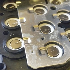
Openair-Plasma from Plasmatreat GmbH is one of the leading technologies worldwide to activate and clean surfaces. It is used in numerous applications to pretreat different substrates. It can also be used to clean metal surfaces for solid wire bonding. The Openair-Plasma technology is a cost-efficient process and can be integrated inline, allowing the bonding process to take place directly after the cleaning is completed.
"Metal can be cleaned using three processes which have different effects and have different treatment goals," says Nico Coenen, Global Business Development Manager Electronics Market of Plasmatreat GmbH, explaining the basic possibilities of plasma treatment. The first process, neutralization, involves the removal of both surface charge and statically bound dirt such as dust particles. This is done by the charge carriers of the Openair-Plasma treatment. In the second process, the volatile components such as moisture and VOCs (volatile organic compounds) are eliminated by evaporation through the thermal effect of the Openair-Plasma treatment. The final cleaning process is removing organic contaminants. The reactive nature of Openair-Plasma causes hydrocarbon chains to be broken down and split into smaller, volatile molecules (up to H2O and CO2).
The successful treatment can be verified, for example, by using an atomic force microscope, which provides visual evidence of the change in the surface. This is a special scanning probe microscope which is used in surface chemistry for mechanical scanning of surfaces and for measuring atomic forces on the nanometer scale. Furthermore, the contact angle method can be used to prove the modified surface tension e.g. by a drop of water. The water drop on the plasma-treated surface changes its wetting properties in such a way that the contact angle and height are reduced and the surface is becoming more hydrophilic.
This is the result of surface cleaning with Openair-Plasma. Especially oxide surfaces, but also contamination caused by bleed out, interfere with the bonding process and prevent reliable connections. Openair-Plasma removes both surface contamination and the oxide layer and the clean surface of the metal alloy is revealed. This is beneficial, in semiconductor applications as particularly clean surfaces are required here in order to reliably bond the ultra-fine wires. The plasma-treated surface allows bonded materials to form a more stable and larger-area connection.
A similar process is used to remove copper oxides, especially in semiconductor and LED applications. By using X-ray photoelectron spectroscopy, the chemical composition of solids and their surface can be determined without causing damage. After treating copper, it can therefore be determined that the surface proportion of copper increases from 3% to 38%, with a concomitant reduction in the carbon content from 43% to 18%. "These changes clearly show that the copper oxide has been reduced and the copper surface area increased," says Coenen. The contact angle analysis also shows a comparable result. Bond wires therefore also form reliable connections here.
In addition to aluminum and copper substrates, nickel surfaces show similarly good properties after being treated with Openair-Plasma. This is particularly important in battery production. Since nickel oxide acts like a barrier layer, which massively complicates the connection with other materials, the cleaning of the nickel surface from oxides is essential. Plasmatreat has therefore developed a special jet for this application that matches the general requirements and at the same time meets the temperature requirements of the process step, for example does not exceed the limit of 50° Celsius.
"The degree to which the individual substrates allow stable wire bonding depends on the material in use. However, the upstream plasma surface treatment improves the application window of the wire bonding process in any case. Both wettability and adhesion are optimized," says Coenen.
Share on:


Testimonial
"Our marketing partnership with I-Connect007 is already delivering. Just a day after our press release went live, we received a direct inquiry about our updated products!"
Rachael Temple - AlltematedSuggested Items
Trouble in Your Tank: Implementing Direct Metallization in Advanced Substrate Packaging
09/15/2025 | Michael Carano -- Column: Trouble in Your TankDirect metallization systems based on conductive graphite are gaining popularity throughout the world. The environmental and productivity gains achievable with this process are outstanding. Direct metallization reduces the costs of compliance, waste treatment, and legal issues related to chemical exposure. A graphite-based direct plate system has been devised to address these needs.
Closing the Loop on PCB Etching Waste
09/09/2025 | Shawn Stone, IECAs the PCB industry continues its push toward greener, more cost-efficient operations, Sigma Engineering’s Mecer System offers a comprehensive solution to two of the industry’s most persistent pain points: etchant consumption and rinse water waste. Designed as a modular, fully automated platform, the Mecer System regenerates spent copper etchants—both alkaline and acidic—and simultaneously recycles rinse water, transforming a traditionally linear chemical process into a closed-loop system.
Driving Innovation: Depth Routing Processes—Achieving Unparalleled Precision in Complex PCBs
09/08/2025 | Kurt Palmer -- Column: Driving InnovationIn PCB manufacturing, the demand for increasingly complex and miniaturized designs continually pushes the boundaries of traditional fabrication methods, including depth routing. Success in these applications demands not only on robust machinery but also sophisticated control functions. PCB manufacturers rely on advanced machine features and process methodologies to meet their precise depth routing goals. Here, I’ll explore some crucial functions that empower manufacturers to master complex depth routing challenges.
Trouble in Your Tank: Minimizing Small-via Defects for High-reliability PCBs
08/27/2025 | Michael Carano -- Column: Trouble in Your TankTo quote the comedian Stephen Wright, “If at first you don’t succeed, then skydiving is not for you.” That can be the battle cry when you find that only small-diameter vias are exhibiting voids. Why are small holes more prone to voids than larger vias when processed through electroless copper? There are several reasons.
The Government Circuit: Navigating New Trade Headwinds and New Partnerships
08/25/2025 | Chris Mitchell -- Column: The Government CircuitAs global trade winds continue to howl, the electronics manufacturing industry finds itself at a critical juncture. After months of warnings, the U.S. Government has implemented a broad array of tariff increases, with fresh duties hitting copper-based products, semiconductors, and imports from many nations. On the positive side, tentative trade agreements with Europe, China, Japan, and other nations are providing at least some clarity and counterbalance.