-

- News
- Books
Featured Books
- smt007 Magazine
Latest Issues
Current Issue
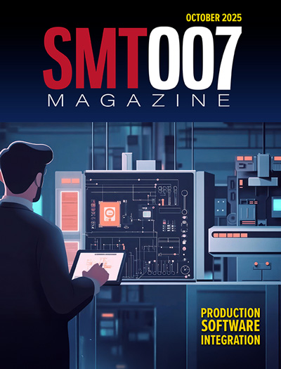
Production Software Integration
EMS companies need advanced software systems to thrive and compete. But these systems require significant effort to integrate and deploy. What is the reality, and how can we make it easier for everyone?

Spotlight on India
We invite you on a virtual tour of India’s thriving ecosystem, guided by the Global Electronics Association’s India office staff, who share their insights into the region’s growth and opportunities.

Supply Chain Strategies
A successful brand is built on strong customer relationships—anchored by a well-orchestrated supply chain at its core. This month, we look at how managing your supply chain directly influences customer perception.
- Articles
- Columns
- Links
- Media kit
||| MENU - smt007 Magazine
Advanced Packaging Gets an Additive Upgrade
November 8, 2022 | Art Wall, NextFlexEstimated reading time: 2 minutes
The recent approval of the CHIPS Act has reignited the U.S. semiconductor industry and shone a spotlight on the intricacies involved in chip manufacturing. As new technological innovations—such as 5G, IoT, AI, automotive and high-performance computing—come to market, they’re pushing chip manufacturing and integration capabilities. They demand more performance which leads to added complexity in an already extremely complicated process. All this requires a fundamental shift in the way that semiconductors are manufactured and integrated.
It's no secret that many believe Moore’s Law, the standard basis for semiconductor innovation over the past 50 years, is reaching the end of its reign. With a need to continue shrinking the size of components, engineers are running into roadblocks based on the physical limitations of electronics manufacturing, packaging, and integration. As manufacturers, we’re tasked with finding new ways of improving electronics capabilities, specifically regarding speed and size.
One of the key strategic avenues that’s arisen is rethinking how we approach the packaging and integration of modern semiconductors. This has implications across the board for chip design, including how they are combined and how they communicate between the chips. Combining dissimilar chips into an integrated package, called heterogeneous integration, and including somewhat generic chip building blocks called chiplets, is quickly becoming necessary to keep pace with technology advancement.
Challenges in Traditional Packaging and Chip Interconnect
Printed circuit boards (PCBs) are the backbone of electronics, acting to connect integrated circuits (ICs) and discrete components to form a larger working circuit. Historically, individually packaged chips and components are mounted to a PCB and interconnected to deliver functionality.
Following this methodology, all the layers in a board act as separate interconnects, leaving the top and bottom of the board to place components. As the drive to miniaturize while simultaneously becoming more complex requires the addition of more components, this is where we’ll begin to see limitations.
An important part of the CHIPS Act was the recognition that not only does the United States need to make massive investments in chip-making facilities or foundries, but also to invest heavily in advanced packaging. Serving as the next step of combining or integrating these chips with novel approaches will be just as important in the innovation of U.S. semiconductor manufacturing capabilities. Some forms of this approach already exist through methodologies such as multi-chip modules or system-in-package (SIP), but more radical approaches are needed to deliver the required performance of the devices.
To read this entire article, which appeared in the November 2022 issue of SMT007 Magazine, click here.
Testimonial
"The I-Connect007 team is outstanding—kind, responsive, and a true marketing partner. Their design team created fresh, eye-catching ads, and their editorial support polished our content to let our brand shine. Thank you all! "
Sweeney Ng - CEE PCBSuggested Items
The Training Connection Continues to Grow with Addition of Veteran IPC Trainer Bill Graver
10/30/2025 | The Training Connection LLCThe Training Connection, LLC (TTC-LLC), a premier provider of test engineering and development training, is proud to announce the addition of Bill Graver to its growing team of industry experts. A respected professional with more than 35 years in electronics manufacturing, Bill joins as an IPC Master Trainer, bringing a wealth of hands-on experience in PCB testing, failure analysis, and process improvement.
I-Connect007 Welcomes New Columnist: Leo Lambert, EPTAC
10/30/2025 | I-Connect007I-Connect007 is excited to announce a column by Leo Lambert, an industry veteran with 40 years of experience, an award winner, and technical director at EPTAC. This column, Learning With Leo, will explore the evolution and related challenges of electronics product assembly, especially as it relates to training.
Cicor to Acquire UK-Based TT Electronics with Board Support
10/30/2025 | Cicor Technologies Ltd.Cicor is a globally active provider of full-cycle electronic solutions (EMS) for the healthcare technology, industrial, and aerospace & defense sectors. TT is a UK-based, London Stock Exchange-listed global provider of engineered electronics for performance critical applications.
Building PCBs and Policy in Europe: Group ACB Champions Advocacy, Standards Development, and Technical Leadership
10/30/2025 | Linda Stepanich, Community MagazineHow does a European PCB manufacturer navigate the competitive manufacturing landscape in Europe? By participating in standards development committee meetings, testifying before the European Commission on industry issues, and sponsoring hand-soldering competitions in the region. Group ACB, based in France and Belgium, focuses on high-reliability applications. The 37-year-old company is also active in the Global Electronics Association, giving credit for helping ACB to raise awareness of electronics manufacturing in Europe.
Highlights at productronica 2025
10/29/2025 | productronicaJust a few more weeks to go before the anniversary edition of productronica. The world’s leading trade fair for the development and production of electronics celebrates its 50th anniversary this fall. From November 18 to 21, Munich will once again be the meeting place for the international electronics industry.


