


 It’s Only Common Sense: The Phone Is Still Mightier Than the Keyboard
 The Marketing Minute: Marketing With Layers


Pusan National University Researchers Develop Way to Tune Energy Levels of Semimetals
March 28, 2023 | PRNewswireEstimated reading time: 2 minutes
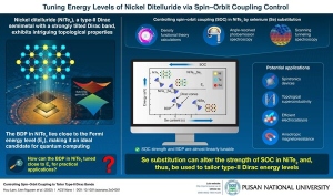
Type-II Dirac semimetals are quantum materials with unique energy level structures, such as a bulk Dirac point (BDP). However, these semimetals are unsuitable for real-life applications because their BDP is far off the "Fermi energy level." Nickel ditelluride (NiTe2), a newly reported type-II Dirac semimetal has a BDP slightly above the Fermi level. Now, researchers have substituted tellurium with selenium in NiTe2 to alter the strength of its spin-orbit coupling and further tune its BDP.
Quantum materials, such as topological semimetals, are materials whose electronic properties are linked to exotic quantum effects. While their interior is a semimetal (e metal with properties between a conductor and semiconductor), the surface behaves like a conductor. This unique electronic behavior arises due to the topology (special geometric properties) of the energy levels occupied by the electrons on the surface of these materials. Specifically, the energy levels closest to the Fermi level (EF)—the highest energy level that an electron can occupy at 0K—form up and down Dirac cones whose tips touch at Dirac points.
Materials with tilted Dirac cones are known as type-II Dirac topological semimetals and have potential applications in topological quantum computing. However, there is a bottleneck. Quantum computers need type-II Dirac semimetals whose bulk Dirac point (BDP) is close to the EF—a rarity. Scientists recently reported that nickel ditelluride (NiTe2) has a BDP slightly above the EF, making it an ideal candidate for quantum computing.
Recently, a research team, led by Associate Professor Jaekwang Lee of Pusan National University, developed a novel technique for further tuning the BDP around the EF in NiTe2. Their work was made available online on 15 July 2022 and published in Volume 16, Issue 7 of the ACS Nano journal on 26 July 2022.
Using density functional theory calculations, the researchers show that substituting tellurium (Te) with selenium (Se) reduces the strength of the spin-orbit coupling (SOC)—the interaction between the electron's spin and its orbital motion around the atomic nucleus—in NiTe2. This shifts the BDP while preserving the type-II Dirac band.
"DFT calculations shows that the SOC strength and the BDP are almost linearly tunable. Scanning tunneling microscopy and angle-resolved photoemission spectroscopy confirm that the BDP in the NiTe2?xSex alloy moves from +0.1 eV (NiTe2) to ?0.3 eV (NiTeSe) about the EF. Further, the BDP is at the exact EF for NiTe1.4Se0.6," highlights Prof. Lee.
Hence, NiTe2?xSex alloys offer a versatile platform for facilitating numerous technologies based on topological effects, including next-generation electronics, spintronics devices, efficient electrocatalysis, topological superconductivity, and quantum computers.
In conclusion, Prof. Lee discusses the longer-term implications of this work. "It provides insights into SOC control to tailor type-II Dirac bands, and will open up new avenues for exploring and developing materials with unconventional electronic properties."
Share on:


Testimonial
"Our marketing partnership with I-Connect007 is already delivering. Just a day after our press release went live, we received a direct inquiry about our updated products!"
Rachael Temple - AlltematedSuggested Items
ITW EAE Despatch Ovens Now Support ASTM 5423 Testing
10/15/2025 | ITW EAEAs the demand for high-performance electrical insulation materials continues to grow—driven by the rapid expansion of electric vehicles (EVs) and energy storage systems—thermal processing has become a critical step in material development.
Beyond Thermal Conductivity: Exploring Polymer-based TIM Strategies for High-power-density Electronics
10/13/2025 | Padmanabha Shakthivelu and Nico Bruijnis, MacDermid Alpha Electronics SolutionsAs power density and thermal loads continue to increase, effective thermal management becomes increasingly important. Rapid and efficient heat transfer from power semiconductor chip packages is essential for achieving optimal performance and ensuring long-term reliability of temperature-sensitive components. This is particularly crucial in power systems that support advanced applications such as green energy generation, electric vehicles, aerospace, and defense, along with high-speed computing for data centers and artificial intelligence (AI).
Is Glass Finally Coming of Age?
10/13/2025 | Nolan Johnson, I-Connect007Substrates, by definition, form the base of all electronic devices. Whether discussing silicon wafers for semiconductors, glass-and-epoxy materials in printed circuits, or the base of choice for interposers, all these materials function as substrates. While other substrates have come and gone, silicon and FR-4 have remained the de facto standards for the industry.
Creative Materials to Showcase Innovative Functional Inks for Medical Devices at COMPAMED 2025
10/09/2025 | Creative Materials, Inc.Creative Materials, a leading manufacturer of high-performance functional inks and coatings, is pleased to announce its participation in COMPAMED 2025, taking place November 17–20 in Düsseldorf, Germany.
Jiva Leading the Charge Toward Sustainable Innovation
09/30/2025 | Marcy LaRont, PCB007 MagazineEnvironmental sustainability in business—product circularity—is a high priority these days. “Circularity,” the term meant to replace “recycling,” in its simplest definition, describes a full circle life for electronic products and all their elements. The result is re-use or a near-complete reintroduction of the base materials back into the supply chain, leaving very little left for waste. For what cannot be reused productively, the ultimate hope is to have better, less harmful means of disposal and/or materials that can seamlessly and harmlessly decompose and integrate back into the natural environment. That is where Jiva and Soluboard come in.