


 The Chemical Connection: Onshoring PCB Production—Daunting but Certainly Possible
 It’s Only Common Sense: The Phone Is Still Mightier Than the Keyboard


Keysight Enables Advanced Pre-Tapeout Silicon Prototyping Using Digital Twin Signaling
May 11, 2023 | Business WireEstimated reading time: 2 minutes
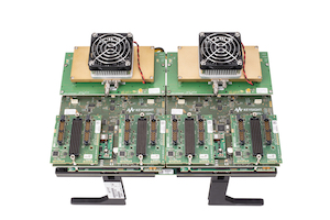
Keysight Technologies, Inc. released a new Universal Signal Processing Architecture (USPA) prototyping platform, enabling semiconductor companies to conduct complete chip prototyping and verification, pre-tapeout, in a real-time development environment integrating digital twins of fully-compliant, standards-based signals.
The final step of the chip design process, known as the silicon tapeout, is an increasingly expensive procedure that leaves little room for design failure. If a design fails following the tapeout, chip makers must start over again with a new “re-spin” that can take 12 months or longer to complete. In addition to tying up valuable research and development resources, these chip redesigns can potentially cause the chip maker to miss a narrow time-to-market window.
To reduce the risks of design failures and expensive re-spins, the Keysight USPA platform provides chip designers and engineers with complete digital twin signaling to verify designs before they are committed to silicon. The USPA platform offers designers an alternative to proprietary custom prototyping systems by integrating ultrafast signal converters with a high performance, completely modular field-programmable gate array (FPGA) prototyping system.
The unique USPA prototyping platform offers the following benefits:
- Supports the highest performance optoelectronic development projects with digital-to-analog converter (DAC) and analog-to-digital converter (ADC) interfaces that emulate signals at full speed, up to 68 GS/s (ADC) and 72 GS/s (DAC).
- Provides a broad range of input / output interfaces that are suitable for applications including 6G wireless development, digital radio frequency memory, advanced physics research, and high-speed data acquisition applications, such as radar and radio astronomy.
- Offers flexibility with two configurations, including a pre-configured system for single channel transceiver applications and a fully configurable set of modular components that can be combined to support a wide range of single and multi-channel applications. In addition, the pre-configured system can be expanded with additional components that leverage the modularity, scalability, and cost-effective reusability of the platform architecture.
Hong Jiang, CEO Avance Semi, Inc., said: “When we began work on our first ASIC for the coherent fiber communication market, we understood that we might only have one chance to get it right and that a second tapeout would be both prohibitively expensive and so time-consuming that we could miss our narrow time-to-market window. With Keysight’s USPA platform and our system integration effort, we can optimize and verify our design in real-time as it progresses. This is like a ‘free soft tapeout’ we can run as many times as needed. This approach saves development time and money while dramatically increasing confidence in our design and product release timeline.”
Dr. Joachim Peerlings, Vice President and General Manager of Keysight’s Network and Data Center Solutions Group, said: “By accelerating and de-risking chip development, Keysight USPA delivers a new end-to-end solution that meets the challenges of leading-edge designs in a very high-cost environment. This powerful platform gives chip developers a digital twin of their future silicon device, allowing them to fully validate their designs and algorithms before incurring the expense and risk of a tapeout.”
Share on:


Testimonial
"Our marketing partnership with I-Connect007 is already delivering. Just a day after our press release went live, we received a direct inquiry about our updated products!"
Rachael Temple - AlltematedSuggested Items
Peters, Starteam, and Würth Elektronik Team Up For Digital Coating Technology
10/23/2025 | PetersUnder this heading, the PCB manufacturers Starteam and Würth Elektronik, along with Peters as inkjet coating supplier, have taken the initiative and worked together for months in trusting and target-oriented cooperation, to promote this innovative digital coating technology for solder resists and establish it on the market.
AI Triggers Next Paradigm Shift in PDN
10/23/2025 | Istvan Novak, SamtecArtificial intelligence (AI), together with machine learning (ML), is creating an unprecedented surge of computing and networking infrastructure needs. This, in turn, has dramatically increased the power consumption of computing and networking chips.
SEMICON Japan 2025 to Spotlight Sustainability in AI and Semiconductor Innovation
10/22/2025 | SEMISEMICON Japan 2025, the largest gathering of leaders from the microelectronics manufacturing supply chain in Japan, will bring together more than 1,200 exhibitors showcasing semiconductor solutions from December 17-19 at Tokyo Big Sight.
Zuken Announces ZIW Americas 2026 in Dallas
10/21/2025 | ZukenZuken USA, Inc., a global leader in electrical and electronic design automation, announced Zuken Innovation World (ZIW) Americas 2026, the company’s premier global conference dedicated to advancing the future of electrical and electronic product design. ZIW 2026 will be held June 9-11 in Dallas, Texas.
Keysight Completes Acquisition of Synopsys’ Optical Solutions Group and Ansys’ PowerArtist
10/17/2025 | Keysight Technologies, Inc.Keysight Technologies, Inc., announced the completion of its acquisitions of the Optical Solutions Group from Synopsys, Inc., and PowerArtist from Ansys, Inc.