-

- News
- Books
Featured Books
- smt007 Magazine
Latest Issues
Current Issue
Moving Forward With Confidence
In this issue, we focus on sales and quoting, workforce training, new IPC leadership in the U.S. and Canada, the effects of tariffs, CFX standards, and much more—all designed to provide perspective as you move through the cloud bank of today's shifting economic market.

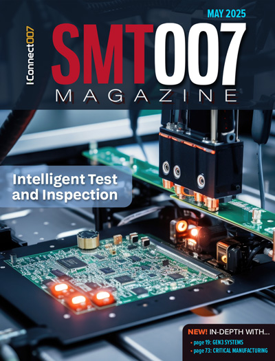
Intelligent Test and Inspection
Are you ready to explore the cutting-edge advancements shaping the electronics manufacturing industry? The May 2025 issue of SMT007 Magazine is packed with insights, innovations, and expert perspectives that you won’t want to miss.

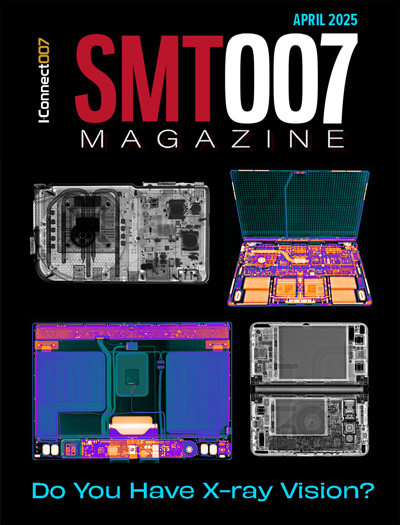
Do You Have X-ray Vision?
Has X-ray’s time finally come in electronics manufacturing? Join us in this issue of SMT007 Magazine, where we answer this question and others to bring more efficiency to your bottom line.
- Articles
- Columns
- Links
- Media kit
||| MENU - smt007 Magazine
Using the Area Ratio Calculator for Stencil Design
May 15, 2006 |Estimated reading time: 3 minutes

 Michael R. Burgess William E. Coleman PhD
<?xml:namespace prefix = o ns = "urn:schemas-microsoft-com:office:office" />
Photo Stencil
In the SMT assembly process, it has been claimed(1) that 40-60% of defects are related back to the printing process. There are many factors that can cause these defects including the stencil, the solder paste, PCB board finishes, stencil printer set-up, squeegee speed, board separation speed, board design and stencil design to name a few. This is by no means a complete list. The issue addressed here is what can be done at the stencil design level to minimize printing defects. All too often, a bad aperture design can cause printing defects resulting in opens, insufficients or shorts. Overlooking this during the stencil design / ordering process is very costly in yield loss during SMT assembly and stencil redesign costs. A good way to check stencil / aperture design is the Area Ratio Calculator(2). A stencil vendor can make recommendations using this calculator. The design / process engineer can do a design check using the calculator.
The stencil printing process can be conveniently divided into three categories: (1) the aperture fill process, (2) the paste transfer process, and (3) the positional location of the deposited paste. All three processes play a vital role in achieving the desired result: a precise volume of paste (referred to as a brick) deposited to the correct location on the substrate. Again, this analysis is further narrowed down considering the relationship of paste transfer and stencil design.
After filling the stencil aperture with solder paste the PCB is separated from the stencil. The intent is to transfer all the paste in the aperture to the PCB pad. However during this transfer a competing process comes into play: will the paste stick to the side aperture walls or will it release to the pad on the PCB? The surface of the pad under the aperture is pulling the paste out of the aperture but the inside walls are holding onto the solder paste. Who wins this tug of war depends on the area ratio as well as the sidewall smoothness.
The area ratio is defined as the area of the aperture opening divided by the area of the inside aperture wall. The smaller the area ratio the more difficult it is to achieve efficient paste transfer. The generally accepted rule is for area ratios greater than .66, acceptable paste transfer is achieved. E-Fab* (electroform) stencils have very smooth aperture walls as seen from the picture below which shows a laser-cut sidewall and an electroformed sidewall. Consequently it has been found that the area ratio can be reduced to .50 and still achieve acceptable paste transfer.

 Laser-Cut Stencil E-FAB Electroform stencil
An example of the area ratio calculator is shown in the chart below:

Stencil design for two devices is shown in the above example; a .5mm uBGA and 0201 chip component. Five different possible designs are shown for each device. For the .5mm uBGA three designs are acceptable. Two designs (with area ratio's of .521 and .550 respectively) recommend a electroform E-Fab stencil with a 5 mil thick foil and one design (with a .688 area ratio) recommends a laser or E-Fab stencil with a 4 mil thick stencil. It is interesting to note that a 6 mil stencil is unacceptable for both devices, a 5 mil stencil recommends an E-Fab stencil and a 4 mil stencil recommends E-Fab or laser stencil. The above illustration of the area ratio calculator is static but an interactive version (Excel based) is available at www.photostencil.com/arearatio.
(1) "Mass Imaging Performance with Lead-free Solder" Clive Ashmore, SMT Mgazine November 2004
(2) "Step by Step Printing" William Coleman, SMT Magazine April 2002
* E-FAB(R) is a patented process of Xerox and licensed to Photo Stencil


